Parts list
This is the full list of parts read from Naya's public FCC filings for the Create halves, the
Speedlink dongle and the Tune, Touch and Track modules, with the unconfirmed readings kept apart
from confirmed part numbers, and the open hardware questions with what would settle each. The same list is published as a data file,
parts.json. The one thing to know: every photographed unit is a
pre-production sample the lab received on 2025-06-20, so retail boards may differ.
At a glance
- 222 main rows: 199 confirmed and 16 corrected by a blind re-read, plus 7 new rows from the exhibits obtained on 2026-09-23 (one extraction pass).
- 21 identified part numbers, 20 boards, 47 unconfirmed readings, 26 open questions.
- Nothing was opened for this list: it reads only public FCC exhibits, vendor manuals and datasheets.
- Candidates in the unconfirmed table are reasoning, never part numbers.
- Data file and page are CC BY 4.0; the facts come from public records.
What the list is and how it was verified
The list was built from the FCC exhibits in 25 extraction passes and then checked by 16 adversarial passes that re-read every cited crop blind and gave each row a verdict; the method is described on Board inventory DOC. When it was built it had 215 main rows (199 confirmed, 16 corrected), 21 identified part numbers, 48 unconfirmed readings, 50 rejected readings and 27 open questions across 20 board entries. The 16 exhibits obtained on 2026-09-23 add 7 rows (LB-20 left label, LB-21 dongle label, LB-22 confidentiality letters, LB-23 dongle SAR report, LB-24 left-half RF-exposure report, DG-19 dongle antenna position, ACC-08 SAR extension cable), settle one unconfirmed reading (U-LB-04b, the ISED numbers) and one open question (OQ-25, the missing exhibits), and extend about 20 rows: 222 main rows, 47 unconfirmed readings, 50 rejected readings and 26 open questions now. The 7 new rows had one extraction pass, not the blind re-read DOC1.
Verdicts: confirmed (a blind re-read found the same marking and the identity holds), corrected (the re-read found a different or fuller value, which the row now carries), unverifiable (kept only in the unconfirmed table), refuted (dropped from the list), and new for the 2026-09-23 rows DOC. The list reads only public FCC exhibits and vendor manuals and datasheets; no hardware was opened for it DOC. The page and the data file are licensed CC BY 4.0 like the rest of the site; the underlying facts come from public FCC records2.
How to read a row
Each row carries an ID, the location on the board, the part, the maker, the function, the marking as read (verbatim, followed by a legibility mark [clear], [partial] or [illegible]), the source (FCC ID, exhibit and lab attachment page, as explained on Regulatory records), the basis (tag and verdict) and notes DOC. The sections are: identifiers and marks; board inventory; half mainboard; wing; dock (thumb-key) board; module dock interface; half enclosure, switches, keycaps and mechanics; dongle; Tune main board; Tune disc, dial and enclosure; Touch main board; Touch sensor, pogo and enclosure; Track main board; Track sensors, pogo, interposer, motor and enclosure; batteries and ratings; accessories in the box DOC.
A "candidate" in the unconfirmed table is reasoning and never a part number: for example a Winbond
W25Q family and capacity for the flash, a C&K PCM12-class slide switch, NAYA-700-3 for the Tune
base, WS2812/SK6812 for the LEDs, CST3640 for the Tune disc DOC INFERRED. Rows measured on hardware read
measured on one <unit>, <firmware>, <date>. The list contains no serial number, serial-number
template value, lab sample number or QR payload: where a label has a serial field, the row says that
the field exists and gives no value DOC.
The published data file
parts.json holds the same rows as this page: boards,
part_number_index, parts (fields id, section, location, part_number, manufacturer,
function, marking, verdict, verdict_note, tag, source, notes, image, image_source), unconfirmed,
open_questions, exhibits (the citation codes) and counts. Compared with the working file behind it, this edition:
- drops every research-run field (verification pass pointers, local file names, inputs, per-row comparisons) and carries no private references;
- corrects two rows from the dongle report's text layer: the dongle's filing is "2 Mbps only" (not
1M / 2M / 125k), and its power setting is 8 / 7 / 8 across 2402 / 2442 / 2480 MHz; the half SoC's
first marking line is published as
N528…(partial) DOC1; - applies the 2026-09-23 exhibits to the rows they touch: the grant dates and grant lines now come from FCC EAS (LB-02a/b/c), all three ISED numbers (LB-04), the left half's KC and MIC numbers and the dongle's placeholders (LB-05, LB-06), the marks on the left and dongle labels (LB-07 to LB-13), the left label exhibit (LB-15), the SAR test software (LB-19), the 0.59 dBi in the left half's MPE report (HM-12), the dongle's exterior photos (DG-15, DG-18), its 5 V 30 mA rating (BAT-20), the left enclosure marks (EN-10 to EN-13), the lab cable (ACC-02) and the dongle's one troubleshooting line (ACC-03) DOC1;
- states the three-way disagreement on module capacities in BAT-16 (website 1500 / 800 / 800, v1.1.0 manuals 1500 / 1500 / 700, filed 1000 / 700 / 600 mAh) instead of the website figures alone DOC;
- extends HM-14: the right-half crop also shows a
D+label and one beginningUS(the left half'sUSB), so both halves most likely carry the same debug and USB test-pad set;D-is still not seen on either DOC INFERRED; - rewords PD-09, PD-10 and PD-11 after the paper-clip test (below), and moves EN-06 (the end cap as the RF window) from INFERRED to DOC on the vendor's own statement MEASURED DOC34.
Already answered since the list was built: the half's dock magnets are real magnets, 6 per bay, the 2 features beside the contacts (PD-11) and the 4 blocks on the carrier plate (PD-10); the 5 blocks on the bay bracket (PD-09) did not attract a steel paper clip MEASURED (owner's board, 2026-09-23) INFERRED. OQ-13 stays open for the module bases.
About the images
The photos on this page and the other hardware pages are crops of Naya B.V.'s FCC exhibits, which are public records on apps.fcc.gov (grantee code 2BQ4V). Identifying marks were removed before publication: QR and 2D codes, serial numbers and serial-number fields, lab sample tags and handwriting are blurred or blacked out, while part markings and board silkscreen are left legible. Each image cites its FCC ID and exhibit: board views in their caption, part crops in the title shown when the image is opened. A row without a crop of its own shows its board instead, and a dash means there is nothing to photograph (report text, USB descriptors, manual text). Click any image to zoom DOC1.
Boards
| Board | Image | Name | Marking as read | Verdict | Row |
|---|---|---|---|---|---|
| Left half mainboard | 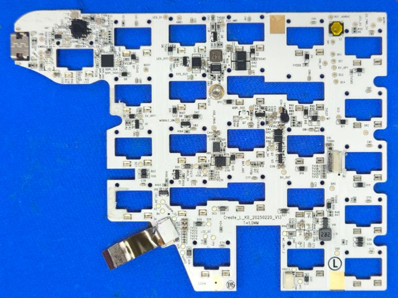 |
Create_L_KB_20250220_V13 |
Create_L_KB_20250220_V13 / T=1.0MM, circled L, on both faces [clear] |
confirmed | HM-01 |
| Right half mainboard | 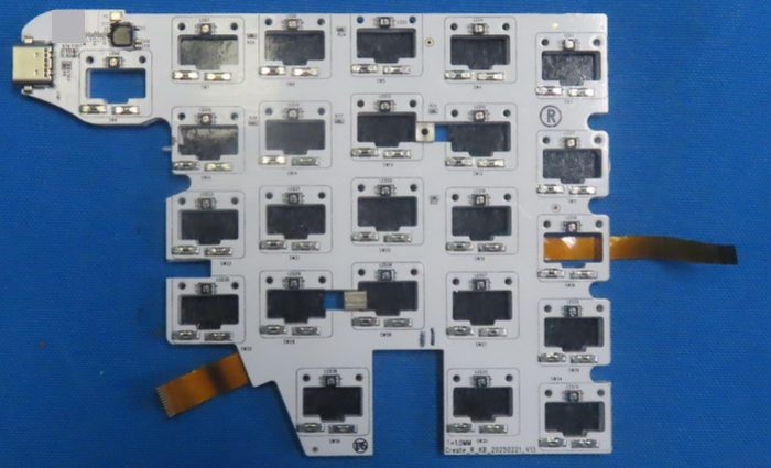 |
Create_R_KB_20250221_V13 |
Create_R_KB_20250221_V13 / T=1.0MM, circled R [clear] |
confirmed | HM-02 |
| Left wing board | 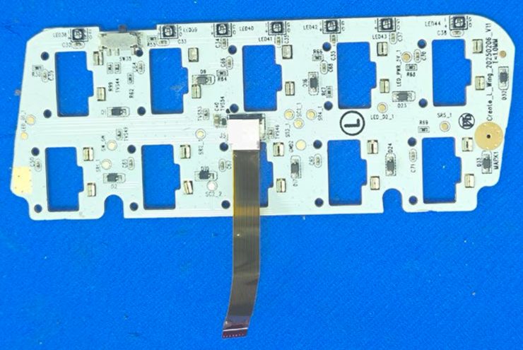 |
Create_L_Wing_20250206_V11 |
Create_L_Wing_20250206_V11 / T=1.0MM [clear]; separate stamp 25 15 [clear] |
confirmed | WG-01 |
| Right wing board | 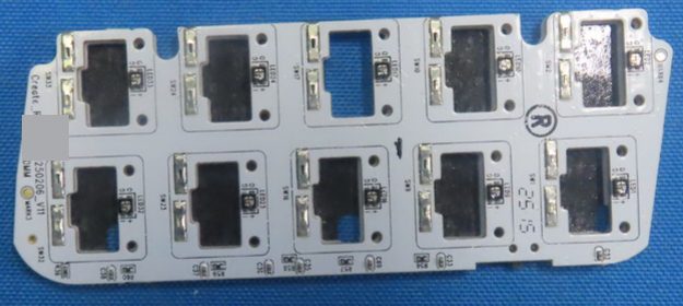 |
Create_R_Wing_20250206_V11 (middle INFERRED) |
Create_R ... 0250206_V11, 1.0MM; _Wing_2 hidden under a QR label; fiducial MARK3 beside [partial] |
confirmed | WG-02 |
| Left dock (thumb-key) board | 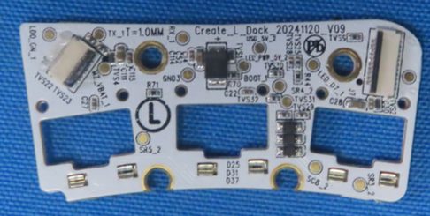 |
Create_L_Dock_20241120_V09 |
Create_L_Dock_20241120_V09 / T=1.0MM, circled L, struck-through Pb (lead-free) circle [clear] |
corrected | DK-01 |
| Right dock board | 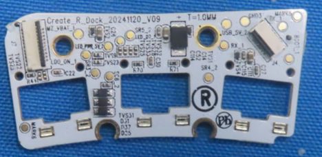 |
Create_R_Dock_20241120_V09 |
Create_R_Dock_20241120_V09 / T=1.0MM, circled R, MARK5, MARK6, Pb-free circle [clear] |
confirmed | DK-02 |
| Left pogo board | 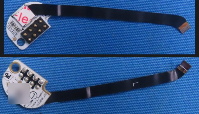 |
Create_L_PogoPin_20250109_V10 |
Create_L_PogoPin / 20250109_V10, T=0.6MM, circled L, Pb-free circle, QR label [clear] |
confirmed | PD-01 |
| Dongle board | 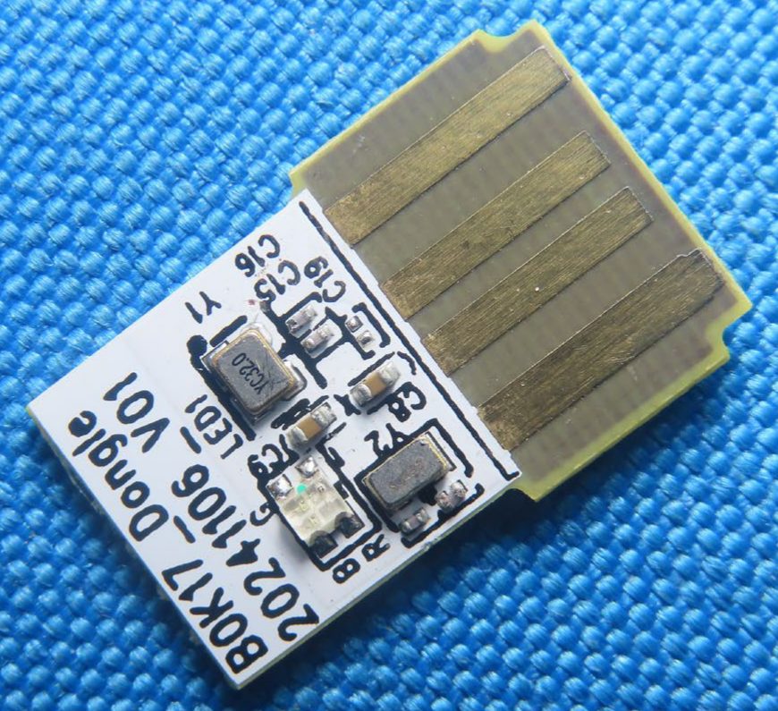 |
B0K17_Dongle_20241106_V01 |
Silkscreen B0K17_Dongle / 20241106_V01 [clear]; report text layer spells the second character as digit zero (U+0030) |
confirmed | DG-01 |
| Tune main board (ring) | 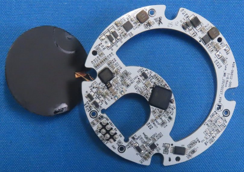 |
Tune_MB_20250227_V09, part no. 408-06032-000 |
Tune_MB_20250227_V09 / 408-06032-000 / T=0.8mm on both faces, Pb-free circle, stamp 25 12, chevron fab logo [clear] |
confirmed | TUM-01 |
| Tune touch/LED disc | 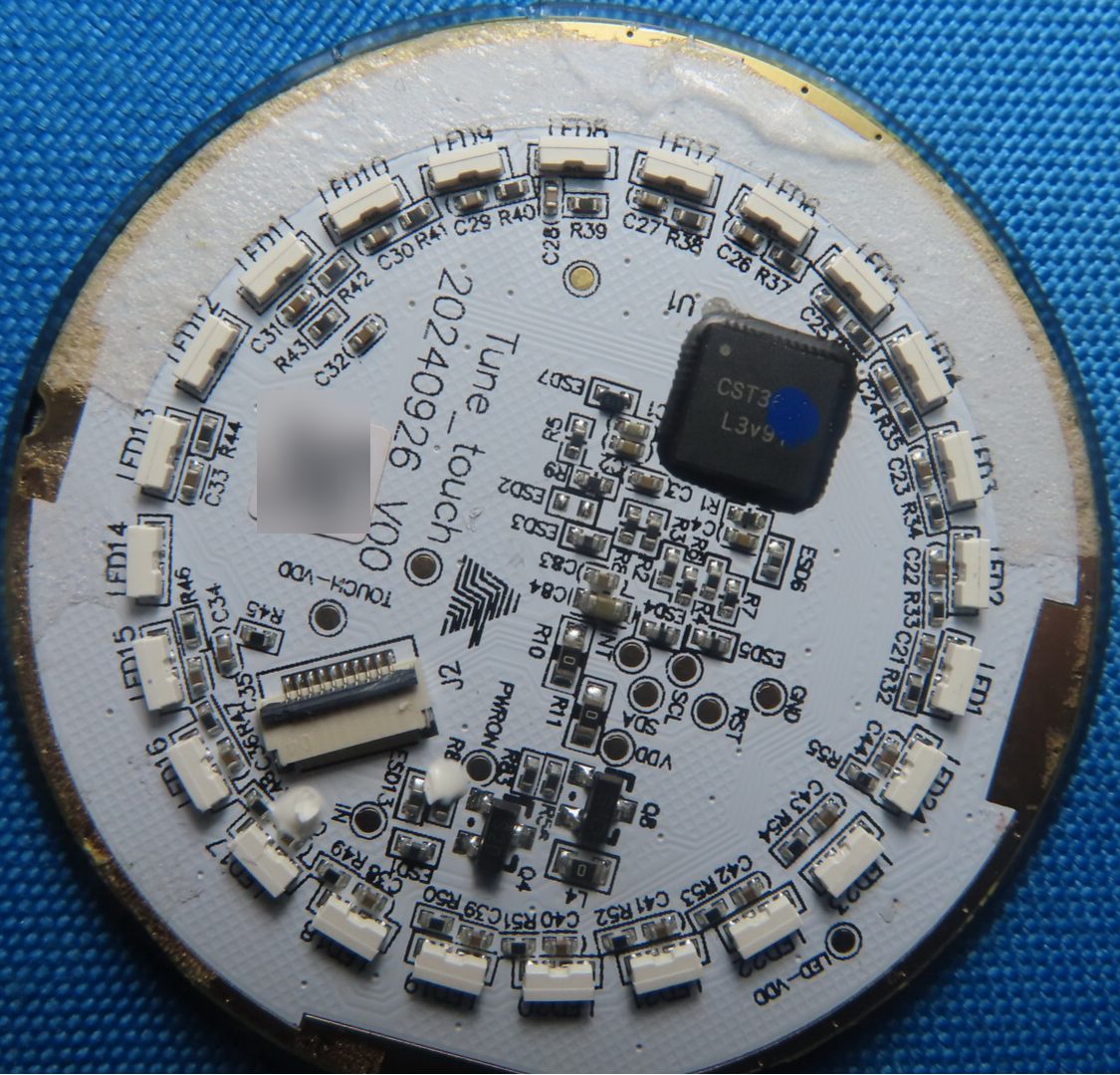 |
Tune_touch 20240926 V00 |
Tune_touch / 20240926 / V00 (lower-case 'touch'), chevron logo, gold edge ring [clear] |
confirmed | TUX-01 |
| Touch main board | 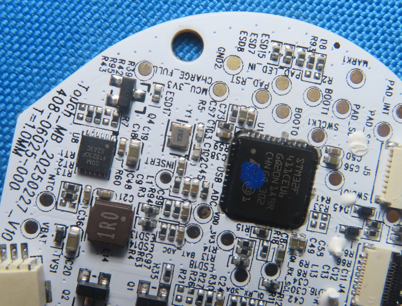 |
Touch_MB_20250227_V10, part no. 408-06025-000 |
Touch_MB_20250227_V10 / 408-06025-000 / T=1.0MM on three lines, Pb-free, chevron logo [clear] |
confirmed | TCM-01 |
| Touch sensor board | 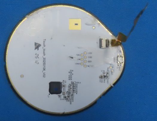 |
Touch_touch_20250106_V02 |
Touch_touch_20250106_V02, stamp 25 12, chevron logo [clear] |
confirmed | TCX-01 |
| Touch pogo board | 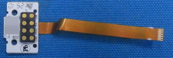 |
Touch_Pogo_Pin_<date>_V0x (INFERRED from the Track name) |
Tou...in / 20...V0? (middle under a 2D sticker); stamp 25 10; Pb-free, chevron logo [partial] |
confirmed | TCX-08 |
| Track main board (ring) | 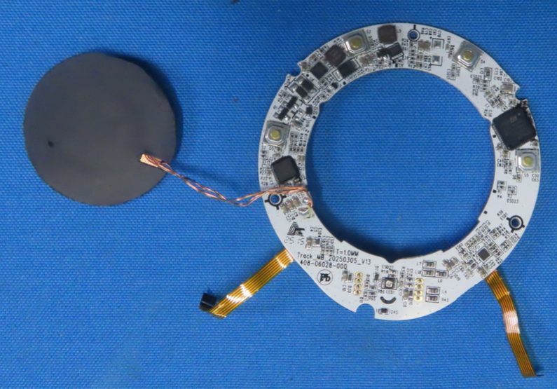 |
Track_MB_20250305_V13, part no. 408-06028-000 |
408-06028-000 / Track_MB_20250305_V13 / T=1.0MM, Pb-free, stamp 25 15, chevron logo [clear] |
confirmed | TKM-01 |
| Track sensor board, left | 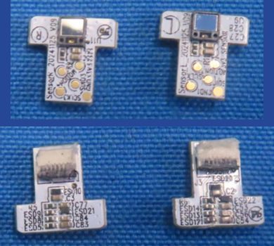 |
SensorL_20241125_V09 |
SensorL_20241125_V09, circled L [clear] |
confirmed | TKX-01a |
| Track sensor board, right | |
SensorR_20241125_V09 |
SensorR_20241125_V09, circled R, Pb-free [clear; R glyph faint] |
confirmed | TKX-01b |
| Track pogo board | 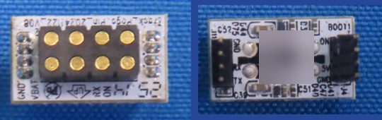 |
Track_Pogo_Pin_20241122_V08 |
Track_Pogo_Pin_20241122_V08, Pb-free; date stamp 25 1? [name clear; stamp partial] |
corrected | TKX-05 |
| Track dock interposer board | |
no name visible | J11 4-pin male header (GND, RX, TX + 1 unlabeled pin); J4 4-pin header (ON, 5V, GND + 1 unlabeled); BOOT1 pad; C39, C47, C51, C52, D40, D44 (partial), D75; QR sticker [clear except where marked] |
confirmed | TKX-09 |
| Right pogo board name | 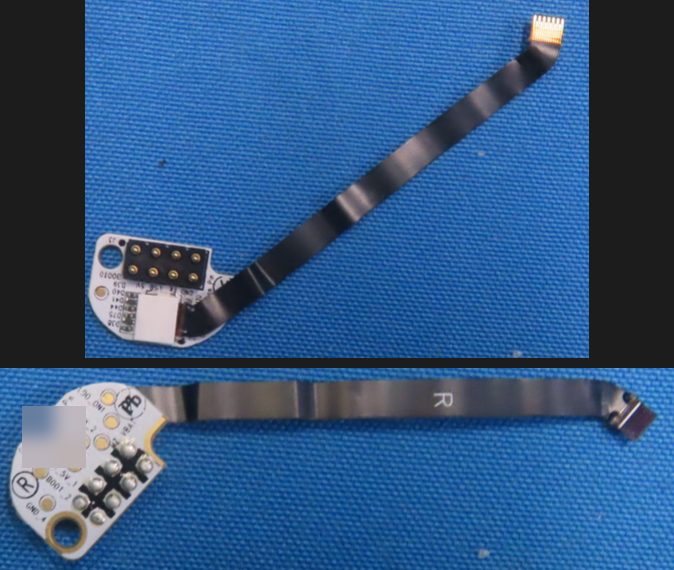 |
- | Circled R, Pb mark, GND_4, BOOT_2, 5V_1, RX_2; name under a QR sticker; Cr / Pin / 10 fragments very low confidence; edge text ?0010 |
unverifiable | U-PD-02 |
| T-shaped sub-board | 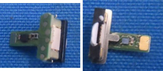 |
- | Green PCB about 10 x 7-9 mm; metal frame about 9.3 x 3.7 mm with a white 'pill' about 3.3 x 1 mm at one end of a slot; 6 pads on the crossbar; about 1.2-1.5 mm unmarked IC; no board name | unverifiable | U-TUX-16 |
Part-number index
Confirmed identities only, one row per part; the Rows column points to the full rows below DOC.
| Part | Maker | Function | Where | Rows |
|---|---|---|---|---|
| nRF52840, CKAA (WLCSP), build D0 | Nordic Semiconductor | BLE SoC | Both halves (U2), dongle (U1) | HM-04, DG-04 |
| Serial NOR flash, P/N unread | Winbond | External QSPI flash | Both halves (U1) | HM-09 |
| RF0400A | Boen | PCB antenna, 0.8 dBi | Both halves | HM-12 |
| RF0401A | Boen | PCB antenna, 3.11 dBi | Dongle | DG-09 |
| CPG-1232 (Kailh PG1232) | Kailh | Low-profile key switch | Both halves, spares | EN-01, ACC-06 |
| STM32F411CEU6 | STMicroelectronics | Module MCU | Tune, Touch, Track | TUM-03, TCM-03, TKM-03 |
| MT5705 | Maxic Technology | Qi 5 W receiver | Tune, Touch, Track | TUM-04, TCM-05, TKM-05 |
SGM41523 (base variant, 41523DF) |
SG Micro | 1-cell switch-mode charger | Tune, Touch, Track (U8) | TUM-05, TCM-06, TKM-06 |
SGM62117 (01KGH) |
SG Micro | Buck-boost converter | Tune (U6), Touch (U3) | TUM-06, TCM-09 |
| CST3640 | Hynitron | Capacitive touch controller | Touch sensor board (Tune: candidate, U-TUX-03) | TCX-02 |
MMBT3904 class (1AM) |
multi-source | NPN transistor | Tune Q3, Touch Q4 | TUM-10, TCM-12 |
B5819W / 1N5819W class (SL) |
multi-source | Schottky 40 V 1 A | Tune, Touch, Track | TUM-11, TCM-13, TKM-11 |
1N4148W / 1N4148WS class (T4) |
multi-source | Switching diode | Tune, Touch, Track | TUM-12, TCM-17, TKM-11 |
100 uF 6.3 V tantalum (J107) |
not identified | Bulk capacitor | Tune, Touch | TUM-14, TCM-15 |
YC32.0 32 MHz crystal |
not identified | HFXO | Halves, dongle | HM-07, DG-06 |
YC16.0 16 MHz crystal |
not identified | STM32 HSE | Tune, Touch, Track | TUM-15, TCM-10, TKM-07 |
FH301217 3.7 V 50 mAh 0.185 Wh |
not identified | Half cell | Each half | BAT-01 |
FH 202030 3.7 V 1000 mAh 3.7 Wh |
not identified | Tune pack | Tune | BAT-06 |
FH364046 / FH364045 3.7 V 700 mAh 2.59 Wh |
not identified | Touch cell(s) | Touch | BAT-09, BAT-10 |
QS801630 1S2P 3.7 V 600 mAh 2.22 Wh (2 x 300 mAh) |
not identified | Track pack | Track | BAT-13, BAT-14 |
NAYA-800-1(NAYA-CREATE); NAYA-100-1(Dongle) |
Naya B.V. | Model numbers | Halves; dongle | LB-01, DG-17a |
The tables, board by board
Each table follows one section of the data file. The accessories rows include the 1 m USB-C Y-cable
(jacket print 30V, VW-1, a temperature rating and a partly legible style number: a UL AWM-class
cable, INFERRED); the lab used a 0.8 m unshielded USB cable without ferrite, which is not the retail
cable DOC INFERRED.
Identifiers, grants and certification marks
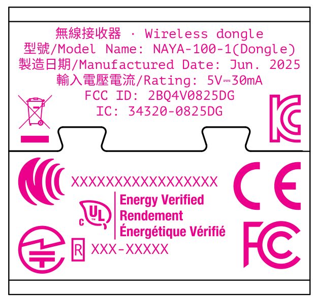
Both halves and the dongle. Label artwork: right half CRR LBL, left half CRL LLOC, dongle DG LBL. Rows LB-20 to LB-24 come from the exhibits obtained on 2026-09-23 (one extraction pass).
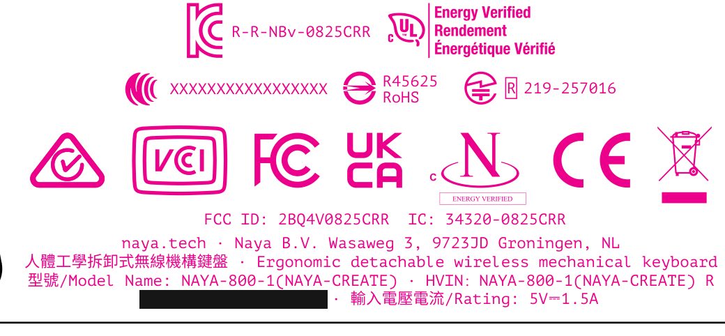
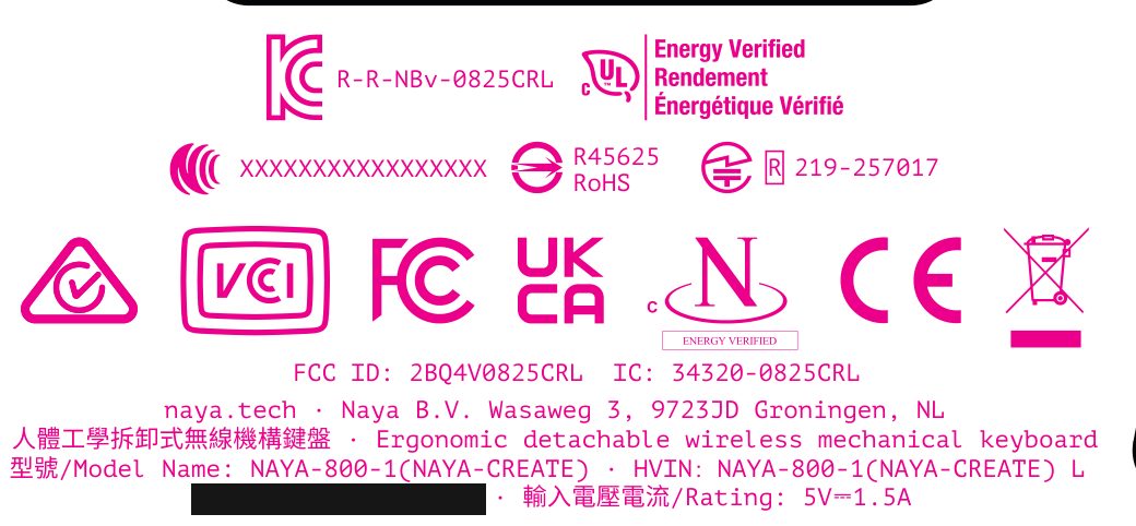
| ID | Image | Location | Part | Maker | Function | Marking as read | Source | Basis | Notes |
|---|---|---|---|---|---|---|---|---|---|
| LB-02a |  |
Grant, left half | FCC ID 2BQ4V0825CRL |
Grantee Naya B.V. (grantee code 2BQ4V) | Naya Create left half; 47 CFR 15.247 DTS, 2402-2480 MHz GFSK, BLE 1M / 2M / 125k (S=8); max peak 9.30 dBm (2M), max average 7.14 dBm (1M); BTL project 2506C291 | Report cover FCC ID: 2BQ4V0825CRL [clear]; grant date 2025-08-26 |
CRL BLE p1, p10; CRL SRD p1; grant date and grant lines from FCC EAS (read 2026-09-23) | DOC; confirmed (Grant date confirmed on FCC EAS (2026-09-23); this ID has two grant lines, 2402-2480 and 2404-2480 MHz) | The SRD report BTL-FCCP-2-2506C291 carries the same FCC ID: it is a second 15.247 report inside this grant, not a second grant. Report R01 issued 2025-08-27, after the grant (R00 was superseded for the antenna gain). The left half's RF-exposure report is BTL-FCCP-3-2506C291 R00 (LB-24). |
| LB-02b |  |
Grant, right half | FCC ID 2BQ4V0825CRR |
Grantee Naya B.V. | Naya Create right half; 15.247 DTS 2402-2480 MHz; max peak 8.36 dBm (2M), max average 7.25 dBm (1M); BTL project 2506C430; RF-exposure report BTL-FCCP-3-2506C430 R01 (SAR-exclusion calculation) | Report cover and label FCC ID: 2BQ4V0825CRR [clear]; grant date 2025-08-29 |
CRR BLE p1, p10; CRR LBL; CRR MPE p1; grant date and grant lines from FCC EAS (read 2026-09-23) | DOC; confirmed | - |
| LB-02c |  |
Grant, dongle | FCC ID 2BQ4V0825DG |
Grantee Naya B.V. | Speedlink dongle; 15.247 DTS 2402-2480 MHz GFSK, tested at 2 Mbps only; 8.97 dBm (2M); BTL project 2506C290; RF report R00 issued 2025-08-12; antenna report BTL-OTA-1-2506C290 R00 | Report cover FCC ID: 2BQ4V0825DG [clear]; grant date 2025-09-03 |
DG RF p1, p10, p11 (EUT table and test modes: 2 Mbps only); grant date and grant lines from FCC EAS (read 2026-09-23) | DOC; corrected (PHY corrected 2026-09-23: the dongle report tests 2 Mbps only (was '1M / 2M / 125k')) | SAR report BTL-FCC SAR-1-2506C290 R00 (LB-23); ISED 34320-0825DG. |
| LB-01 |  |
Model / HVIN, both halves | NAYA-800-1(NAYA-CREATE) |
Naya B.V. (brand 'NAYA TECH, Naya Create') | One model number for both halves, told apart by FCC ID suffix (CRL/CRR); equipment 'Ergonomic detachable wireless mechanical keyboard' | Label Model Name: NAYA-800-1(NAYA-CREATE), HVIN: NAYA-800-1(NAYA-CREATE) followed by R (right-half marker) [clear]; reports 'Keyboard: Left Keyboard' |
CRR LBL; CRL BLE p1, p10; CRR BLE p1; CRR UM1 p1; CRR UM5 p1 | DOC; confirmed | The left label reads HVIN NAYA-800-1(NAYA-CREATE) L (LB-20); ISED lists both HVINs with the side suffix. |
| DG-17a |  |
Model, dongle | NAYA-100-1(Dongle) |
Naya B.V. | Speedlink dongle, equipment 'Wireless dongle' | Test Model: NAYA-100-1(Dongle) [clear]; manual box list subtitle 'Wireless dongle · NAYA-100-1(Dongle)' |
DG RF p1, p10; CRR UM1 p2 | DOC; confirmed | - |
| LB-04 | 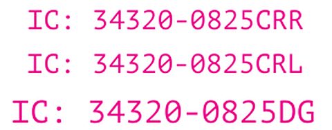 |
ISED Canada, right half | IC: 34320-0825CRR; 34320-0825CRL; 34320-0825DG |
ISED company number 34320 | Canadian radio certification number | IC: 34320-0825CRR on the same line as the FCC ID [clear] |
CRR LBL; CRR UM5 p2 (IC statements, no number); CRL LLOC p1; DG LBL; ISED REL (read 2026-09-23) | DOC; confirmed | All three numbers are on their label artwork (CRR LBL, CRL LLOC p1, DG LBL) and on the ISED Radio Equipment List for company 34320 (approved 2025-09-11 CRL, 2025-09-08 CRR and DG). |
| LB-05 |  |
Korea KC, right half | R-R-NBv-0825CRR |
Korea RRA (KC mark) | Korean radio certificate | KC mark + R-R-NBv-0825CRR [clear on label artwork]; KC logo also engraved on the left half, its number [illegible]; left label artwork R-R-NBv-0825CRL [clear]; dongle label: KC logo without a number |
CRR LBL; CRL EP p2; CRR EP p2-p3; CRL LLOC p1; DG LBL | DOC; confirmed | - |
| LB-06 | 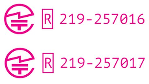 |
Japan MIC, right half | 219-257016 (right), 219-257017 (left) |
MIC technical conformity (Giteki); certification body 219 not identified |
Japanese radio certification: 3-digit body code + 6-digit number, boxed R = radio equipment |
Giteki mark + boxed R + 219-257016 [clear] |
CRR LBL; CRL LLOC p1; DG LBL | DOC; INFERRED (format decode from public MIC guides); confirmed | The two numbers are consecutive (one batch, INFERRED). The dongle label carries only an XXX-XXXXX placeholder. The certification body behind code 219 is not identified. |
| LB-07 |  |
Taiwan BSMI, right half | R45625 |
BSMI (Taiwan) | Commodity-inspection registration with RoHS declaration | Circle-with-arrow mark + R45625 over RoHS [clear, also in the PDF text layer] |
CRR LBL; CRL LLOC p1 | DOC; INFERRED (registrant-level number); confirmed | The same number appears on unrelated Taiwan-market products, so it most likely identifies the importer/registrant, not this product (INFERRED). On the left label as on the right; not on the dongle label. |
| LB-08 |  |
Taiwan NCC-style mark, right half | placeholder XXXXXXXXXXXXXXXXX (17 characters) |
- | Placeholder for an NCC number in the artwork; real NCC numbers are 12-14 characters (INFERRED) | Stylised three-arc mark + 17 X [clear] |
CRR LBL; CRL LLOC p1 | DOC; INFERRED; confirmed | On both half labels and on the dongle label. |
| LB-09 |  |
EU/UK marks, both halves | CE, UKCA, WEEE | - | EU and UK conformity marks; WEEE disposal mark | CE; UK over CA; crossed-out wheelie bin with bar [clear on artwork; faint engraving on both photographed halves] |
CRR LBL; CRL EP p2; CRR EP p2-p3; CRL LLOC p1 | DOC; confirmed | An earlier text search reported CE and UKCA as not found: the marks are vector graphics, invisible to a text search. The dongle label has CE and WEEE, no UKCA. |
| LB-10 |  |
Australia/NZ and Japan EMC marks | RCM, VCCI | - | Supplier-declaration marks, no number printed | Triangle with a tick in a circle; double box with VCI letterforms [clear on artwork; faint on samples] |
CRR LBL; CRL EP p2; CRR EP p3; CRL LLOC p1 | DOC; INFERRED (shape identification); confirmed | On both half labels; not on the dongle label. |
| LB-11 |  |
Energy-verification marks | c-UL 'Energy Verified'; c + N-in-ellipse 'ENERGY VERIFIED' | UL (first mark); issuer of the N mark not identified | Canadian energy-efficiency verification marks | c + UL leaf + 'Energy Verified / Rendement / Énergétique Vérifié'; c + N crossed by an ellipse + boxed 'ENERGY VERIFIED' [clear] |
CRR LBL; CRL LLOC p1 | DOC; confirmed | Both marks on both half labels; the dongle label has the c-UL mark only. |
| LB-12 | 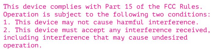 |
FCC statement on the body plate | Part 15 two-condition statement (6 lines) | - | Required FCC label text | 'This device complies with Part 15 of the FCC Rules. Operation is subject to the following two conditions: ...' [clear in artwork text layer]; not visible on the photographed sample | CRR LBL; CRR EP p3; CRL LLOC p1 | DOC; confirmed | The photographed sample probably carried an earlier engraving (INFERRED). On the left body plate as on the right; not on the dongle label (it is in the manual). |
| LB-13 |  |
Half input rating | 5V⎓1.5A |
- | DC input rating of one half | 輸入電壓電流/Rating: 5V⎓1.5A [clear] |
CRR LBL; CRL LLOC p1 | DOC; confirmed | The left label gives the same rating. |
| LB-14 | - | Manual power figures | 'Input Voltage 4.2V'; charge from 'USB 2.0 5V-1A' | - | Spec-sheet power figures; 4.2 V reads as the Li-ion full-charge voltage, not the input (INFERRED; the label rates the input 5 V 1.5 A) | Spec sheet 'Input Voltage 4.2V'; best practices 'connecting the provided USB cable to a computer (USB 2.0 5V-1A)' [clear] | CRR UM1 p3, p5; CRL UM1 p3, p5 | DOC; INFERRED (meaning); confirmed | - |
| LB-15 | 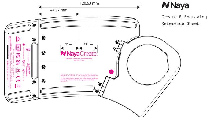 |
Label layout (right half) | 'Create-R Engraving Reference Sheet' | - | 1:1 laser-engraving artwork: regulatory block on the wing underside plate, rotated 90°; logo on the body plate 47.97 mm from the seam; serial-number field (no value reproduced) | Dimension line 120.63 mm (re-measured 120.73 mm at 150 dpi: artwork is 1:1); PDF title 'Create 镭雕-20250820', created 2025-08-20, modified 2025-08-27 | CRR LBL (exhibit R15) | DOC; confirmed | The serial-number field value is not reproduced. The left filing's 'Label Location' exhibit holds both sheets (CRL LLOC p1 left, p2 right; p2 equals the CRR exhibit). |
| LB-16 | - | Manufacturer and test lab | Dongguan Boen Intelligent Technology Co., Ltd.; BTL Inc. (Dongguan) | - | ODM (manufacturer and factory of record for all three filings) and the test lab; also the antenna maker (RF0400A, RF0401A) | Report covers: 'Manufacturer / Factory: Dongguan Boen Intelligent Technology Co., Ltd.'; test facility: FCC registration 747969, designation CN1377; A2LA certificate 7130.01 [clear] |
CRR BLE p1, p8; CRL BLE p1; DG RF p1 | DOC; confirmed | - |
| LB-17 | - | Taiwan RoHS table | CNS 15663-style restricted-substance table | - | Declaration for units Cable, PWAs, Plastic parts, Metal parts, Rubber parts against Pb, Hg, Cd, Cr+6, PBB, PBDE; every cell '○'; no battery row | Table text [clear]; equipment 人體工學拆卸式無線機構鍵盤, type NAYA-800-1(NAYA-CREATE) | CRR UM5 p1; CRL UM3 p5 | DOC; confirmed | - |
| LB-18 | - | USB identity, halves | VID 0x37D1; PID left 0x0064 / right 0x00C8; MCUboot 0x006F / 0x00D3; DFU 0x007A / 0x00DE; generation-B bit 0x1000 |
Naya (VID not in public USB-ID lists) | USB identity of each half in application, MCUboot recovery and DFU modes; bit 0x1000 marks QSPI flash generation B (0x1064 / 0x10C8) |
n/a (USB descriptors); product strings 'Naya Create Left' / 'Naya Create Right' | STATIC: NayaCore 6.11.0 PID table (vendor host binary); measured on one pair of halves, keyboard firmware 3.41.0, generation A, by 2026-09-16 | STATIC (NayaCore 6.11.0); MEASURED (0x0064, 0x00C8, 0x006F on keyboard firmware 3.41.0, generation A); confirmed |
0x00D3 and the DFU pair are STATIC only (not yet seen on hardware). |
| DG-17b | - | USB identity, dongle | VID 0x37D1, PID 0x012C (transient boot identity 0x0137), bcdDevice 0x0307 |
Naya | Dongle USB identity: CDC composite, product string 'Dongle' | n/a (USB descriptors) | measured on one dongle: USB enumeration capture, 2026-09-11 | MEASURED (one dongle, 2026-09-11); INFERRED (bcdDevice 0x0307 read as dongle firmware 3.07); confirmed | - |
| LB-19 | - | Declared EUT software and lab tool | Naya_Temp_Flash_Pair.exe; nrfconnect-setup-5.1.0-x64 |
Naya (EUT software); Nordic (lab tool) | Software version declared for the tested samples (halves and dongle); channel/power control tool = the installer name of nRF Connect for Desktop 5.1.0 (INFERRED), power setting 8 on every channel and PHY for the halves; the dongle table reads 8 / 7 / 8 at 2402 / 2442 / 2480 MHz | 'Software Version Naya_Temp_Flash_Pair.exe'; 'Test Software Version nrfconnect-setup-5.1.0-x64'; power setting tables: halves all 8; dongle 8 7 8 [clear, text layer] |
CRL BLE p10, p13; CRL SRD p10, p12; DG RF p10, p11 | DOC; INFERRED (meaning of the installer name); corrected (Dongle power setting corrected 2026-09-23 from the DG RF p11 text layer (middle channel 7, not 8)) | No keyboard firmware version is printed anywhere in the filings; samples were pre-production units received by the lab on 2025-06-20. The dongle's SAR sample also ran Naya_Temp_Flash_Pair.exe; its continuous transmission came from '2.4G SRD engineering testing software installed on the DUT' (DG SAR p7, p23). |
| LB-20 | |
Left-half label artwork | FCC ID: 2BQ4V0825CRL; IC: 34320-0825CRL; KC R-R-NBv-0825CRL; MIC 219-257017; HVIN NAYA-800-1(NAYA-CREATE) L |
Naya B.V. | 'Create-L Engraving Reference Sheet', 1:1: the regulatory block on the left wing plate underside, mirrored from the right; the same marks, BSMI number, NCC-style placeholder, maker line, serial-number field (no value reproduced) and Part 15 text as the right half; rating 5V⎓1.5A; L circle by the dock hinge; 12 screw symbols |
[clear, vector artwork] | CRL LLOC p1 | DOC; new (2026-09-23 exhibits) (one extraction pass, no blind re-read) | - |
| LB-21 | |
Dongle label artwork | engraving artwork 'Dongle', 2025-07-25, 12.55 x 12.00 mm | Naya B.V. | Text: 'Wireless dongle', Model Name: NAYA-100-1(Dongle), 'Manufactured Date: Jun. 2025', Rating: 5V⎓30mA, FCC ID: 2BQ4V0825DG, IC: 34320-0825DG; marks WEEE, KC without a number, an NCC-style 17-character placeholder, c-UL Energy Verified, a Japanese Giteki mark with an XXX-XXXXX placeholder, CE and FCC. No UKCA, RCM, VCCI, BSMI or N-in-ellipse mark, no address, serial-number field or Part 15 text |
[clear, vector artwork] | DG LBL; DG EP p2-p3 | DOC; INFERRED (1:1 scale from the USB-A shell width; placement); new (2026-09-23 exhibits) (one extraction pass, no blind re-read) | The photographed sample carries no engraving; where on the dongle the label goes is not stated. |
| LB-22 | - | Confidentiality requests (all three IDs) | - | Naya B.V. | Letters dated 2025-08-06 (CRL) and 2025-08-04 (CRR, DG) request confidentiality under 47 CFR 0.457 and 0.459 for exactly the block diagram, schematics and operational description, as trade secrets; no short-term request for any other exhibit, so these three are permanent | [clear, text] | CL (CRL, CRR, DG) | DOC; INFERRED (permanent); new (2026-09-23 exhibits) (one extraction pass, no blind re-read) | - |
| LB-23 | - | Dongle RF exposure | SAR report BTL-FCC SAR-1-2506C290 R00 | BTL Inc. (Dongguan) | Issued 2025-08-12, tested 2025-07-12 to 07-22; EUT NAYA-100-1(Dongle), hardware B0K17_Dongle_20241106_V01, software Naya_Temp_Flash_Pair.exe; mode '2.4G SRD', GFSK, 2M, 2400-2483.5 MHz; RF0401A 3.11 dBi; average conducted 6.28 / 6.60 / 6.71 dBm at 2402 / 2442 / 2480 MHz, tune-up 8.00 dBm; 100 % duty; five positions (horizontal up and down, vertical front and back, tip) at 5 mm; highest reported 1-g SAR 0.080 W/kg (2402 MHz, horizontal down; measured 0.054 scaled to tune-up) against 1.6 W/kg |
[clear, text] | DG SAR p1, p7, p22-p26; DG SAR-D | DOC; new (2026-09-23 exhibits) (one extraction pass, no blind re-read) | - |
| LB-24 | - | Left-half RF exposure | MPE report BTL-FCCP-3-2506C291 R00 | BTL Inc. (Dongguan) | Issued 2025-08-15, never revised: RF0400A filed at 0.59 dBi (the specification table's 2460 MHz value); BLE 7.14 dBm and '2.4G SRD' 4.35 dBm tune-up at 2480 MHz; results 1.630 and 0.858 against 3.0 (1-g SAR exclusion); 'No SAR evaluation required' | [clear, text] | CRL MPE p1-p4 | DOC; INFERRED (reproduced with 5 mm and unrounded mW); new (2026-09-23 exhibits) (one extraction pass, no blind re-read) | - |
PCB inventory: board names, revisions, silkscreens
Every board whose name is legible in the filings. Rows here are not repeated in the per-board tables below. The right pogo board and the Tune T-shaped sub-board have no legible name and are in the Unconfirmed table.
| ID | Image | Location | Part | Maker | Function | Marking as read | Source | Basis | Notes |
|---|---|---|---|---|---|---|---|---|---|
| HM-01 | 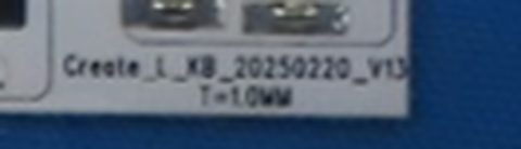 |
Left half mainboard | Create_L_KB_20250220_V13 |
Custom PCB (board house not named; ODM Dongguan Boen) | Left main PCB, 1.0 mm; design date 2025-02-20, revision V13 | Create_L_KB_20250220_V13 / T=1.0MM, circled L, on both faces [clear] |
CRL IP1 p8, p9; declared HW version CRL BLE p10, CRL SRD p10, CRR BLE p10, CRR SRD p10, CRR MPE p1 | DOC; confirmed | Both faces read V13 (V11 is the wing). |
| HM-02 |  |
Right half mainboard | Create_R_KB_20250221_V13 |
Custom PCB | Right main PCB, 1.0 mm; 2025-02-21, V13 | Create_R_KB_20250221_V13 / T=1.0MM, circled R [clear] |
CRR IP1 p6; CRL BLE p10 (the SRD report prints Create_R_KB20250221_V13) |
DOC; confirmed | - |
| WG-01 | 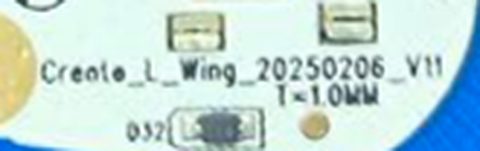 |
Left wing board | Create_L_Wing_20250206_V11 |
Custom PCB | Left wing PCB (outer two key columns), 1.0 mm; 2025-02-06, V11 | Create_L_Wing_20250206_V11 / T=1.0MM [clear]; separate stamp 25 15 [clear] |
CRL IP1 p11, p12 | DOC; INFERRED (stamp = fab year 25, week 15); confirmed (Stamp now read in full (was 25 ?5)) |
- |
| WG-02 | 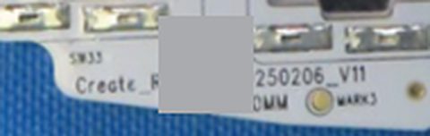 |
Right wing board | Create_R_Wing_20250206_V11 (middle INFERRED) |
Custom PCB | Right wing PCB, 1.0 mm | Create_R ... 0250206_V11, 1.0MM; _Wing_2 hidden under a QR label; fiducial MARK3 beside [partial] |
CRR IP1 p9 | DOC (legible part); INFERRED (hidden part, from the left twin); confirmed | - |
| DK-01 | 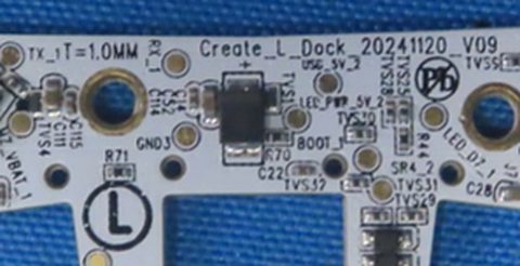 |
Left dock (thumb-key) board | Create_L_Dock_20241120_V09 |
Custom PCB | Board under the module bay carrying the three thumb keys and the dock signals; 1.0 mm; about 47 x 21 mm (INFERRED) | Create_L_Dock_20241120_V09 / T=1.0MM, circled L, struck-through Pb (lead-free) circle [clear] |
CRL IP2 p16; CRL IP1 p5, p7 (low resolution) | DOC; corrected (No separate 'UL-like' mark: that was the Pb-free circle seen at low resolution) | - |
| DK-02 | 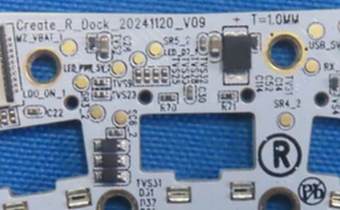 |
Right dock board | Create_R_Dock_20241120_V09 |
Custom PCB | Right dock board, 1.0 mm | Create_R_Dock_20241120_V09 / T=1.0MM, circled R, MARK5, MARK6, Pb-free circle [clear] |
CRR IP1 p12 | DOC; confirmed | - |
| PD-01 | 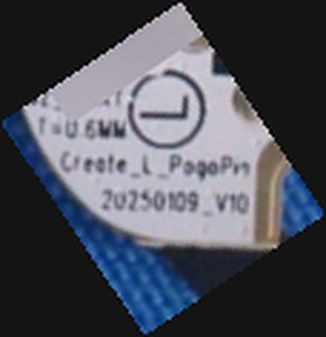 |
Left pogo board | Create_L_PogoPin_20250109_V10 |
Custom PCB | D-shaped board carrying the half's 8 dock spring pins; 0.6 mm; about 16 x 17 mm (INFERRED) | Create_L_PogoPin / 20250109_V10, T=0.6MM, circled L, Pb-free circle, QR label [clear] |
CRL IP2 p15; CRL IP1 p5, p7 | DOC; confirmed | - |
| DG-01 | 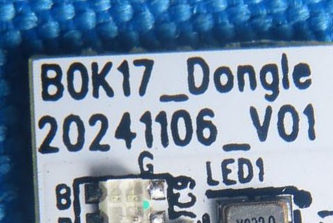 |
Dongle board | B0K17_Dongle_20241106_V01 |
Custom PCB | Dongle PCB, 2024-11-06, V01; double-sided, stepped outline about 16.5-18 x 10-11.6 mm (INFERRED) | Silkscreen B0K17_Dongle / 20241106_V01 [clear]; report text layer spells the second character as digit zero (U+0030) |
DG IP p4, p5; DG RF p10 | DOC; confirmed | - |
| TUM-01 | 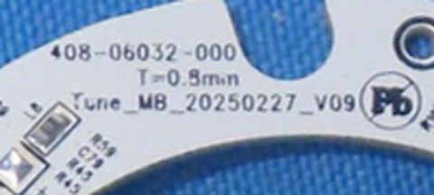 |
Tune main board (ring) | Tune_MB_20250227_V09, part no. 408-06032-000 |
Custom PCB | Tune ring PCB about 58-60 mm across with a C-shaped inner island (INFERRED size); 0.8 mm | Tune_MB_20250227_V09 / 408-06032-000 / T=0.8mm on both faces, Pb-free circle, stamp 25 12, chevron fab logo [clear] |
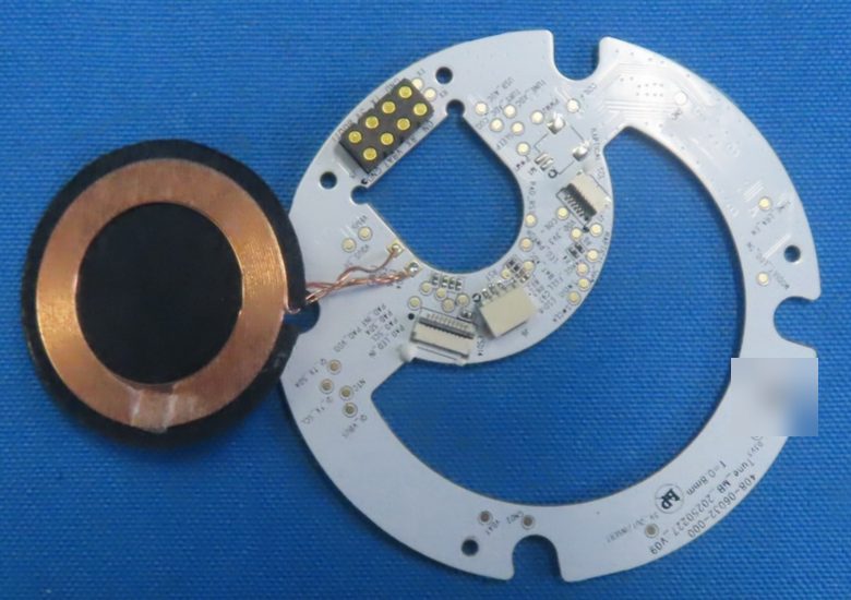
CRL IP2 p18; CRL IP3 p19, p21 = CRR IP2 p15-p16; CRR IP3 p18 | DOC; INFERRED (stamp = 2025 week 12); confirmed | 408-060xx-000 is one numbering series with the Touch (06025) and Track (06028) main boards (INFERRED). |
| TUX-01 | 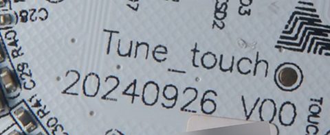 |
Tune touch/LED disc | Tune_touch 20240926 V00 |
Custom PCB | Round disc about 45 mm bonded under the glass: touch controller and 24-LED ring | Tune_touch / 20240926 / V00 (lower-case 'touch'), chevron logo, gold edge ring [clear] |
CRL IP2 p18; CRL IP3 p22; CRL IP4 p23 = CRR IP2 p15; CRR IP3 p19-p20 | DOC; confirmed | - |
| TCM-01 | 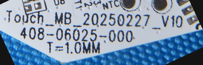 |
Touch main board | Touch_MB_20250227_V10, part no. 408-06025-000 |
Custom PCB | Round, about 44 mm (anchored to the 7 x 7 mm STM32 package), single-sided, 1.0 mm | Touch_MB_20250227_V10 / 408-06025-000 / T=1.0MM on three lines, Pb-free, chevron logo [clear] |
CRL IP4 p28; CRL IP5 p29-p31 = CRR IP4 p25-p27; CRR IP5 p28 | DOC; INFERRED (size); confirmed | - |
| TCX-01 | 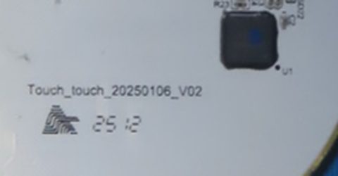 |
Touch sensor board | Touch_touch_20250106_V02 |
Custom PCB | Teardrop capacitive sensor board, diamond-lattice electrodes, gold edge ring; size unresolved (U-TCX-16b) | Touch_touch_20250106_V02, stamp 25 12, chevron logo [clear] |
CRL IP4 p28; CRL IP6 p35-p36 = CRR IP4 p25; CRR IP5 p32-p33 | DOC; confirmed | - |
| TCX-08 | 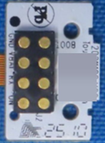 |
Touch pogo board | Touch_Pogo_Pin_<date>_V0x (INFERRED from the Track name) |
Custom PCB | Module-side dock contact board, about 11 x 16.5-18 mm (INFERRED) | Tou...in / 20...V0? (middle under a 2D sticker); stamp 25 10; Pb-free, chevron logo [partial] |
CRL IP4 p28; CRL IP5 p32 = CRR IP4 p25; CRR IP5 p29 | DOC (fragments); INFERRED (full name); confirmed (Only the fragments are confirmed) | - |
| TKM-01 | 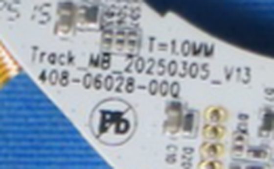 |
Track main board (ring) | Track_MB_20250305_V13, part no. 408-06028-000 |
Custom PCB | Track ring PCB about 60-66 mm OD with a 40-43 mm opening for the 40 mm ball (INFERRED); 1.0 mm | 408-06028-000 / Track_MB_20250305_V13 / T=1.0MM, Pb-free, stamp 25 15, chevron logo [clear] |
CRL IP7 p44-p46 = CRR IP6 p41; CRR IP7 p42-p43 | DOC; INFERRED (size, stamp = 2025 week 15); confirmed | - |
| TKX-01a | 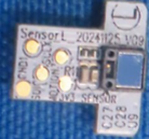 |
Track sensor board, left | SensorL_20241125_V09 |
Custom PCB | T-shaped rigid board about 11 x 11 mm carrying optical ball sensor U9 (optical INFERRED from SCLK/SDIO/MOTION pads) |
SensorL_20241125_V09, circled L [clear] |
CRL IP6 p38-p39 = CRR IP6 p35-p36 | DOC; INFERRED (function); confirmed | - |
| TKX-01b | 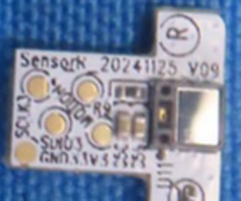 |
Track sensor board, right | SensorR_20241125_V09 |
Custom PCB | Twin of SensorL carrying optical sensor U11 | SensorR_20241125_V09, circled R, Pb-free [clear; R glyph faint] |
CRL IP6 p38-p39 = CRR IP6 p35-p36 | DOC; INFERRED (function); confirmed | Two sensor boards, not four: each is photographed front and back. |
| TKX-05 | 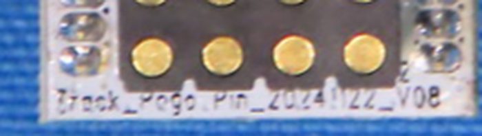 |
Track pogo board | Track_Pogo_Pin_20241122_V08 |
Custom PCB | Module-side dock contact board, about 17 x 10 mm (INFERRED) | Track_Pogo_Pin_20241122_V08, Pb-free; date stamp 25 1? [name clear; stamp partial] |
CRL IP6 p38, p40 = CRR IP6 p35, p37; CRL IP6 p37 = CRR IP5 p34 (in the base) | DOC; corrected (Revision V08 confirmed on three views; the stamp's 14 reading is not confirmed (U-TKX-05b)) |
- |
| TKX-09 | 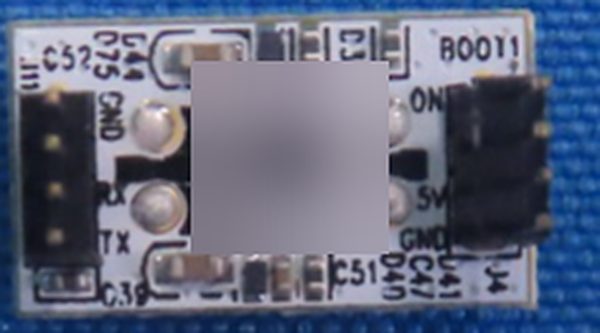 |
Track dock interposer board | no name visible | Custom PCB | Separate small board between the pogo contacts and the main board's two 4-way sockets | J11 4-pin male header (GND, RX, TX + 1 unlabeled pin); J4 4-pin header (ON, 5V, GND + 1 unlabeled); BOOT1 pad; C39, C47, C51, C52, D40, D44 (partial), D75; QR sticker [clear except where marked] |
CRL IP6 p40 = CRR IP6 p37 (upper photo) | DOC; confirmed | A dark SOT/DFN part sits in the lower row; its U41 refdes is not legible (U-TKX-09b). |
Keyboard half mainboard (Create_L_KB_20250220_V13, Create_R_KB_20250221_V13)
Left and right are mirror designs; one row covers both boards unless it says otherwise. Photos: left CRL IP1 p7-p10, right CRR IP1 p6-p8 (the SoC and flash close-up is CRR IP1 p8, which is PDF page 4 of that file).
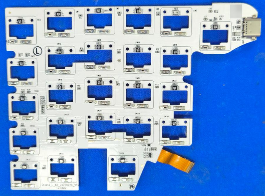
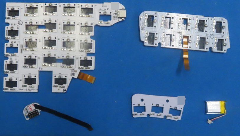
| ID | Image | Location | Part | Maker | Function | Marking as read | Source | Basis | Notes |
|---|---|---|---|---|---|---|---|---|---|
| HM-04 | 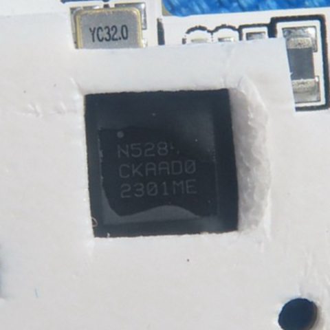 |
U2, both halves, under a cut-out in white foam |
nRF52840, package code CKAA (WLCSP, about 3.5 x 3.6 mm; about 4 mm with underfill), build code D0 | Nordic Semiconductor | BLE SoC: 2.4 GHz radio, native USB 2.0 full-speed device, 1 MB flash, 256 KB RAM, QSPI host | N528… / CKAAD0 / 2301ME on both halves [line 1 partial: N528 plus one or two partly hidden glyphs; lines 2-3 clear] |
CRL IP1 p10 (two close-ups), p7, p9; CRR IP1 p8; transmit data CRL BLE p13, CRR BLE p13 | DOC (marking; CKAA = nRF52840 WLCSP per distributor listings); INFERRED (D0 = Revision 2); confirmed (Identity rests on package code CKAA, conducted power and native USB with no second MCU, not on line 1; one verification pass read line 1 as N52840 after gamma correction) |
Build code D0 matches Nordic's Revision 2 pattern; Revision 3 (hardened APPROTECT) uses Fx0 (INFERRED from Nordic DevZone; confirm in Nordic's revision document, OQ-05). Same lot 2301ME as the dongle. Conducted peak 8.2-9.3 dBm at power setting 8 is above an nRF52811's +4 dBm (INFERRED). |
| HM-07 | 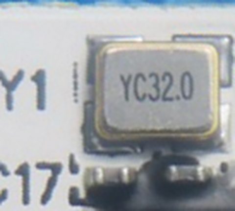 |
Y1, both halves, beside U2 |
32.000 MHz crystal, 4-pad metal lid, about 2.0 x 1.6 mm (2016 class) | not identified (YC prefix; no marking-database match) |
nRF52840 32 MHz HFXO (radio clock) | YC32.0 [clear] |
CRL IP1 p10, p7; CRR IP1 p8 | DOC (marking); INFERRED (size); confirmed | Same marking on the dongle (DG-06). |
| HM-09 | 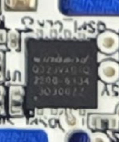 |
U1, both halves, at the USB-C corner |
not read (Winbond serial NOR flash; W25Q family INFERRED from a Q on line 2) |
Winbond | External QSPI NOR flash on the nRF52840 QSPI bus | Right: line 1 winbond [clear], lines 2-4 [illegible to partial, see U-HM-09b]; left: square leadless IC beside QSPI_CLK [illegible]; package 8-pad leadless USON/WSON class, about 4 mm square, not SOIC-8 |
CRR IP1 p8; CRL IP1 p9 | DOC; confirmed (Maker and package confirmed; part number unverifiable) | Part number and capacity unverifiable (U-HM-09b, U-HM-10). The package is leadless, so a SOIC-8 clip does not fit; only the Winbond wordmark is confirmed (no W25Q suffix, no capacity). |
| HM-11 | 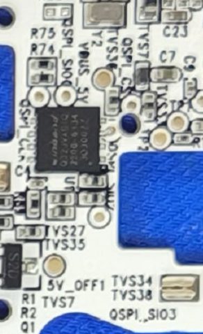 |
QSPI test pads beside U1 | test pads | - | nRF52840 QSPI bus to U1 | Left: QSPI_CS, QSPI_CLK, QSPI_SIO0, QSPI_SIO1; right: QSPI_CS?, QSPI_CLK, QSPI_SIO0, QSPI_SIO3 [clear except the right CS suffix] |
CRL IP1 p9; CRR IP1 p8 | DOC; corrected (Right-half SIO digits now legible (were SIO? x2)) |
- |
| HM-12 | 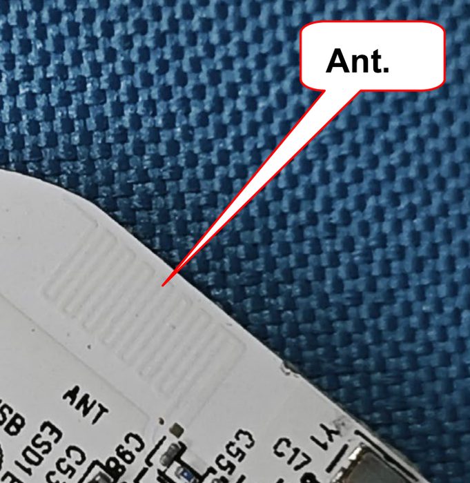 |
ANT, both halves, rear-inner corner beside USB-C |
RF0400A (spec ver1.1) | Boen (Dongguan Boen Intelligent Technology Co., Ltd.) | 2.4 GHz printed meander PCB antenna, connector N/A; peak 0.8 dBi at 2400 MHz; -0.3 to 0.8 dBi and 46.1-63.0 % efficiency over 2400-2480 MHz; trace 7.8 x 3.2 mm (spec drawing) | Silkscreen ANT; lab callout 'Ant.'; spec header 'keyboard antenna RF0400A specification ver1.1'; filed 'BOEN RF0400A PCB N/A 0.8' [clear] |
CRL ANT p1 (table), p4 (drawing); CRR ANT; CRL IP1 p7; CRR EP p3; CRL BLE p11; CRR BLE p11; CRR MPE p4; CRL MPE p4 | DOC; confirmed | Sits behind the black end cap (EN-06; the vendor confirms the cap is the RF window). The spec's 'Directivity' column equals minus efficiency in dB (spreadsheet error). The R01 reports file 0.8 dBi (the 2400 MHz maximum); the left half's MPE report R00, never revised, files 0.59 dBi (the 2460 MHz value), and the right half's superseded R00 most likely did too (INFERRED). |
| HM-13 | 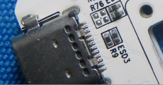 |
USB1, rear-inner corner facing the other half |
USB Type-C receptacle, unmarked | not identified | Half USB port: power and USB 2.0 full-speed data | No marking; oval metal shell, through-hole shell legs, a row of SMT legs [clear shape] | CRL IP1 p6, p7, p9; CRR IP1 p8; CRL EP p4; CRR EP p4; CRR UM1 p6 | DOC; confirmed | 16-pin vs 24-pin class not resolvable (U-HM-13b). |
| HM-14 | 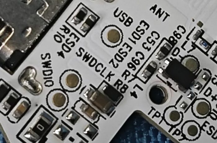 |
SWD and USB test pads at the USB-C corner | test pads | - | nRF52840 Serial Wire Debug; USB D+ test point | Left: SWDIO, SWDCLK, TP1, TP7, USB, D+; right: SWDIO, SWDCLK, TP2 [clear]; D- not visible in any crop |
CRL IP1 p7, p9; CRR IP1 p8 | DOC; confirmed | A re-view of the right-half crop (2026-09-23) also shows a D+ label and one beginning US on the right, so both halves most likely carry the same debug and USB test-pad set; D- is still not seen on either. |
| HM-15 | 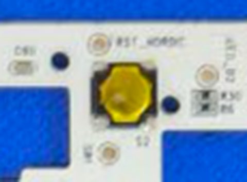 |
S2 and pads RST_NORDIC, BOOT |
tactile switch, yellow cap, unmarked | not identified | nRF52840 reset button; BOOT pad function not documented |
S2, RST_NORDIC, BOOT [clear; BOOT may read BOOT1, U-HM-15b] |
CRL IP1 p9; CRR IP1 p7 (switch through a window, no refdes) | DOC; confirmed | The silkscreen RST_NORDIC names the SoC vendor. |
| HM-16 | 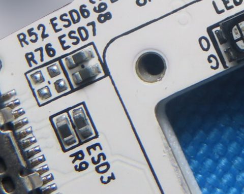 |
USB, VBUS and CC protection around USB1 | ESD/TVS parts, unmarked | not identified | ESD and surge protection on USB and VBUS; L1/L4 beside U2 are probably the nRF DC/DC and RF-match positions (INFERRED) |
Refs (subset per half): ESD1-ESD11, TVS7, TVS27, TVS34, TVS35, TVS37, TVS38, TVS40, L1, L2, L4, R and C refs, TP2 [refs clear; parts unmarked] |
CRL IP1 p7, p9, p10; CRR IP1 p8 | DOC; confirmed | - |
| HP-01 | 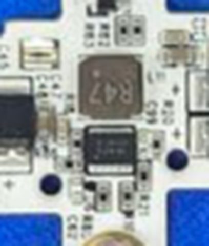 |
L11 (left), with an adjacent unmarked IC |
0.47 uH SMD power inductor (EIA code R47) |
not identified | Switching-regulator inductor (DC-DC 1, INFERRED from the paired IC) | Inductor body R47 [clear]; adjacent 4-6 pad IC with pin-1 dot [illegible] |
CRL IP1 p9 | DOC; corrected (Value is a direct decode of the printed EIA code (was tagged INFERRED)) | The IC is U-HP-01b. |
| HP-02 | 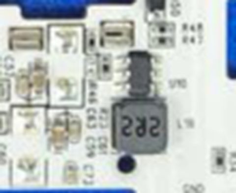 |
L10 (left), with U10 |
2.2 uH SMD power inductor (EIA code 2R2) |
not identified | Switching-regulator inductor (DC-DC 2, INFERRED) | Inductor 2R2 [clear]; U10 6-lead SOT-23-6 [illegible] |
CRL IP1 p9 | DOC; corrected (Value decoded from the printed code) | U10 is U-HP-02b. |
| HP-05 | 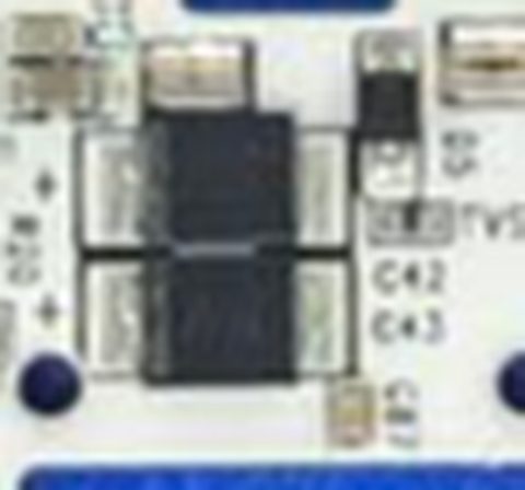 |
C42, C43 (left), beside TVS45 |
polarised molded chip capacitors (tantalum or polymer class) | not identified | Bulk capacitance | Refs C42, C43; + printed on each case; end band [clear]; no value code |
CRL IP1 p9 | DOC; confirmed | - |
| HP-09 | 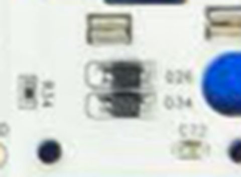 |
Diode and TVS arrays (left) | small signal diodes and TVS parts, unmarked | not identified | Key-matrix diodes and line protection | D3-D47 and TVS3-TVS88 (subsets) [refs clear; parts unmarked] |
CRL IP1 p8, p9 | DOC; confirmed | - |
| HP-11 | 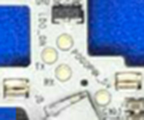 |
Pads at the dock-flex exit (left) | test pads | - | Half-to-module UART, 5 V pogo rail, module LDO enable (roles from the names) | LDO_ON, TX, RX, POGOPIN_5V [clear] |
CRL IP1 p9 | DOC; INFERRED (roles); confirmed | Full dock net set: PD-13. |
| HP-12 | 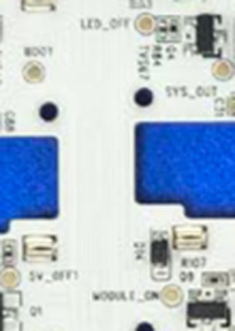 |
Power and rail test pads | test pads | - | Switched module, LED and 5 V rails; ADC sense points (INFERRED from names) | VBUS_5V, USB_ADC, BAT_ADC, SYS, SYS_OUT, 5V_OUT, 5V_OFF, 5V_OFF1, MODULE_ON, VCC_A?T, CHG_?NT, LED_PWR_5V, LED_OFF, LED_01, LED_02, LED_0?, GND1, GND, INT, MARK1, MARK2 (left); VBUS_5V (right) [clear except ?] |
CRL IP1 p9; CRR IP1 p8 | DOC; confirmed (Subset re-read (5V_OFF1, MODULE_ON, VBUS_5V); rest uncontradicted) |
- |
| HP-13 | 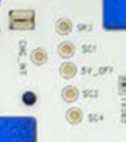 |
Key-matrix test pads | test pads | - | Switch rows (SR) and columns (SC) (INFERRED from names) |
SR1-SR5, SC1-SC6 [clear] |
CRL IP1 p9 | DOC; confirmed | The dock board continues the scheme (SR*_2, SC8_2). |
| HP-14 | 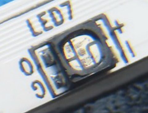 |
Per-key LEDs, 24 per mainboard | addressable RGB LED, 4-pad, unmarked | not identified | Per-key RGB backlight, daisy-chained (no LED driver IC on either face); spec sheet 'Backlighting: Reprogrammable RGB' | Refs LED4, LED6-LED8, LED14, LED15, LED21, LED22, LED29, LED30; pad letters O, G, I, + (right) and -, +, G, O (left) [refs clear; LED body unmarked] |
CRL IP1 p8, p9; CRR IP1 p6; CRR UM1 p3 | DOC (footprint, pads); INFERRED (WS2812/SK6812 class); confirmed | LED part numbers: U-LED. |
| HP-15 | |
LED chain, whole keyboard | - | - | Host LED map, 136 entries per layer: 0-73 keys; 74-80 and 81-87 the two side light bars (7 each); 88-111 left bay block (24); 112-135 right bay block (24) | n/a (host and firmware data) | measured on one keyboard: LED band-painting pass 2026-09-08; LED map size on keyboard firmware 3.41.0 and 3.28.7 | MEASURED (band-painting pass 2026-09-08; map size on keyboard firmware 3.41.0 and 3.28.7); confirmed | Photo count per half: 24 mainboard + 10 wing + 3 dock = 37 key LEDs, plus 7 side-bar LEDs = 44; two halves = 88 = indices 0-87 (INFERRED match). Which physical edge is 74-80 is open (OQ-08). |
| HP-16 | 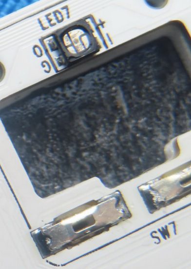 |
Key positions on the mainboard | hot-swap socket footprints (24 per mainboard) | - | 24 hot-swap key positions per mainboard | Refs SW6, SW7, SW14, SW15, SW21, SW22, SW29, SW30, SW35; two socket pads per window [clear] |
CRL IP1 p8, p9; CRR IP1 p6 | DOC; confirmed | Socket part: U-EN-02. |
| HP-17 | 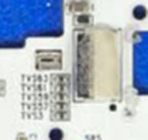 |
Wing FPC receptacle (left), beside TVS53-TVS63 |
flip-lock ZIF/FPC receptacle, unmarked | not identified | Link to the wing board's flex | White/clear ZIF, about 12-14 gold contacts [countable, not exact] | CRL IP1 p9 | DOC; corrected (Way count refined from 'not countable') | - |
| HP-18 | 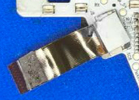 |
Dock-link flex tail at a white board connector (ref consistent with CN3) |
flex cable, unmarked | - | Mainboard to dock board link; right half shows two amber tails (to wing and to dock) | Gold/amber flex, about 12-13 conductors, beside the TX/RX/POGOPIN_5V/LDO_ON pads [clear] |
CRL IP1 p8, p9; CRR IP1 p6, p7 | DOC; INFERRED (destinations); confirmed | - |
| HP-19 | 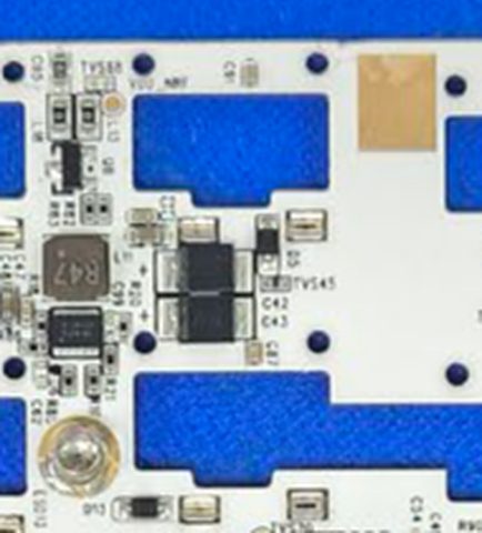 |
Case ground lands (left) | bare gold lands | - | Case or shield ground contact (INFERRED) | Large rectangular gold pad(s); round metal boss near ESD12 (not re-checked) |
CRL IP1 p9 | DOC; INFERRED (function); confirmed | - |
| HP-20 | 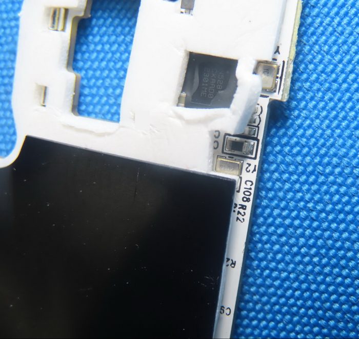 |
Insulation over the component side | black film with windows; white foam layer | - | Assembly insulation; the foam has a rectangular cut-out exactly over U2 | Black film with windows and red handwriting (not transcribed); white foam with cut-out [clear] | CRL IP1 p8, p10; CRR IP1 p7 | DOC; confirmed | - |
Wing board (outer two key columns, Create_L/R_Wing_20250206_V11)
Photos: left CRL IP1 p11-p12, right CRR IP1 p9.
| ID | Image | Location | Part | Maker | Function | Marking as read | Source | Basis | Notes |
|---|---|---|---|---|---|---|---|---|---|
| WG-03 | 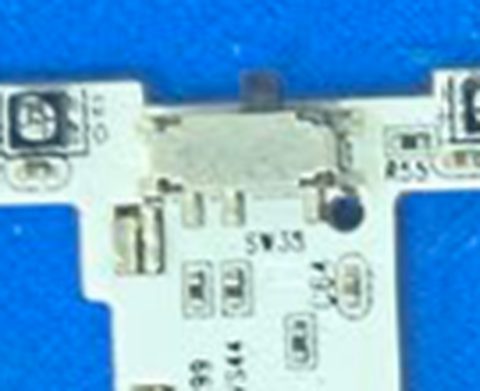 |
Wing outer end face; right wing: between side-bar LEDs 6 and 7 | right-angle SMD slide switch, 3 terminals + 2 tabs, unmarked | not identified | Half power on/off switch ('Locate the power switch on the side of each keyboard wing') | No designator or marking on the switch [clear shape]; white body, gray lever past the board edge (right); the nearby SW33 is a key |
CRL IP1 p12; CRR IP1 p9; CRL EP p4; CRR EP p4; CRR UM1 p5 | DOC; confirmed | ON/OFF direction not determinable (manual drawings CRR UM1 p5 and UM2 p3 disagree). Candidate part: U-WG-03b. |
| WG-04 | 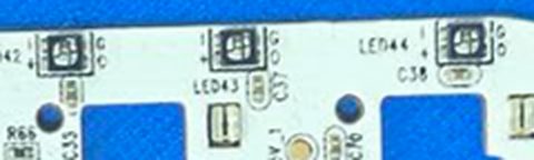 |
Per-key LEDs, 10 per wing | addressable RGB LED, 4-pad, unmarked | not identified | Wing key backlight, same footprint as HP-14 | LED36-LED45 (read LED36, LED38-LED42, LED44); pads O, G, I, + [refs clear] |
CRL IP1 p11, p12 | DOC; INFERRED (class); confirmed | - |
| WG-05 |  |
Side light bar on one long edge of wing face B | 7 addressable 4-pad LEDs | not identified | The half's side light bar (LED indices 74-80 / 81-87) | Exactly 7 LEDs in a row, pads O, G, +; partial ref LED56 at one end; slide switch between the 6th and 7th [clear count] |
CRR IP1 p9; measured on one keyboard (LED map, 7 side-bar indices per half, 2026-09-08) | DOC; MEASURED (7 per side in the LED map, 2026-09-08); confirmed | The left wing's face B is under black film. |
| WG-06 | 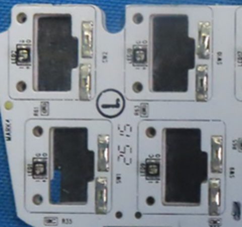 |
Key windows, 10 per wing | hot-swap socket footprints | - | 10 wing key positions, same numbering mirrored on both wings | SW1, SW2, SW9, SW10, SW16, SW17, SW23, SW24, SW32, SW33 on each wing [clear] |
CRL IP1 p11; CRR IP1 p9 | DOC; corrected (Same designators on both wings (was read as right-wing only)) | - |
| WG-07 | 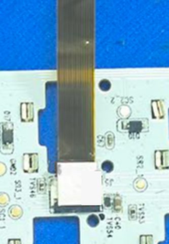 |
Wing flex and connector | flex + FPC connector J5 (left); ZIF in a central window (right) |
not identified | Wing to mainboard link (mates HP-17) | Left: orange/brown flex, about 12 conductors, red/white sticker, into J5; right: small white ZIF [clear] |
CRL IP1 p12; CRR IP1 p9 | DOC; confirmed (New refdes J5) |
- |
| WG-08 | 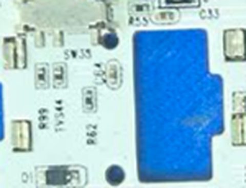 |
Wing passives and fiducials | passives, fiducials | - | Support parts around the slide switch and corners | Left: MARK1, C32, R55, R62, R99, TVS44; right: MARK3, MARK4, resistor cluster R56-R60 [clear] |
CRL IP1 p12; CRR IP1 p9 | DOC; confirmed (R36 not found (Rejected R-40)) |
- |
Dock (thumb-key) board (Create_L/R_Dock_20241120_V09)
Photos: left CRL IP2 p16 (and CRL IP1 p5, p7 at low resolution), right CRR IP1 p12.
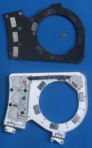
| ID | Image | Location | Part | Maker | Function | Marking as read | Source | Basis | Notes |
|---|---|---|---|---|---|---|---|---|---|
| DK-03 | 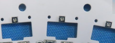 |
Thumb-key LEDs, 3 per dock board | addressable RGB LED, unmarked | not identified | Thumb-key backlight (addressable, INFERRED from LED_D7_1 data and LED_PWR_5V_2 pads) |
Left: 3 black square packages about 2 mm; right: 3 four-pad LEDs on face B; faint 1-2 character top mark [illegible] | CRL IP2 p16; CRR IP1 p12 | DOC; INFERRED (class); confirmed | - |
| DK-04 | 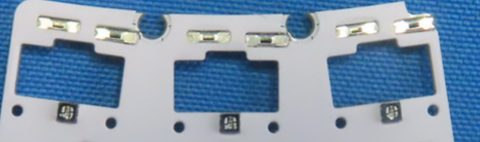 |
Thumb-key positions, 3 per dock board | hot-swap sockets (6 unmarked metal parts, 2 per window) | not identified (Kailh-compatible class INFERRED) | Three hot-swap thumb-key positions | 3 windows, 2 slotted pads each; 6 silver parts about 3 x 1.3 mm on both faces [clear] | CRL IP2 p16; CRL IP1 p7; CRR IP1 p12; CRR UM3 p4 | DOC (manual: 'Hot-Swappable Switches', 'sockets'); INFERRED (the metal parts are the sockets); confirmed | - |
| DK-05 | 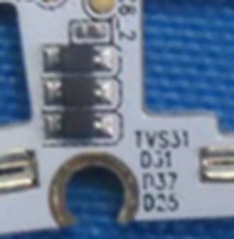 |
D25, D31, D37 |
small signal diodes, unmarked | not identified | One key diode per thumb key (INFERRED) | Three identical unmarked 2-terminal parts beside TVS31 [refs clear] |
CRL IP2 p16; CRR IP1 p12 | DOC; INFERRED (role); confirmed | - |
| DK-06 | 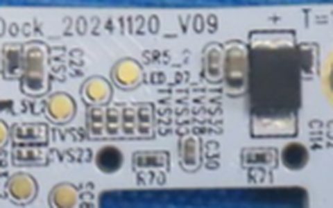 |
TVS array | TVS parts, unmarked | not identified | ESD protection on every dock and key line | TVS1, TVS2, TVS4, TVS5, TVS9, TVS22, TVS23, TVS25, TVS28-TVS32 (union of both boards) [clear] |
CRL IP2 p16; CRR IP1 p12 | DOC; confirmed | - |
| DK-07 | 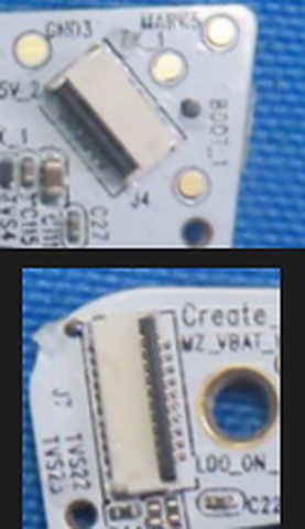 |
FPC connectors: J7 + an unlabeled ZIF (left); J7 + angled J4 (right) |
flip-lock FPC ZIF receptacles, unmarked | not identified | One takes the mainboard flex, one the pogo flex (right: J4 takes the pogo flex, INFERRED from routing) |
Cream/white bodies, gold contact combs, about 10-16 contacts [count not exact] | CRL IP2 p16; CRR IP1 p12 | DOC; INFERRED (mating); confirmed | - |
| DK-08 | 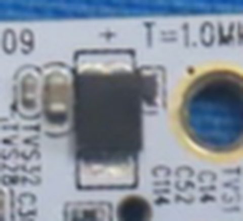 |
Polarised part between TVS1 and R70 |
polarised chip capacitor, tantalum or polymer class, unmarked | not identified | Bulk capacitance | Black molded body, wraparound end terminations, + on the silkscreen above [clear] |
CRR IP1 p12; CRL IP2 p16 | DOC; INFERRED (class); confirmed (Identity narrowed from 'capacitor or diode') | - |
| DK-10 | 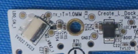 |
Dock-board test pads | test pads | - | UART to the module, boot select, module battery rail, LDO enable, USB-derived 5 V, thumb-key matrix lines, LED data and power | TX_1, RX_1, BOOT_1, MZ_VBAT_1, LDO_ON_1, USB_5V_2, GND3; SR1_2 (partial), SR3_2, SR4_2, SR5_2, SC8_2; LED_D7_1, LED_PWR_5V_2; R70, R71, C14, C22, C27-C30, C52, C111, C114, C115 [clear except where marked]; no D+/D- anywhere |
CRL IP2 p16; CRR IP1 p12 | DOC; INFERRED (roles); confirmed (MZ_VBAT_1 (not M2_VBAT_1) and LDO_ON_1 resolved) |
- |
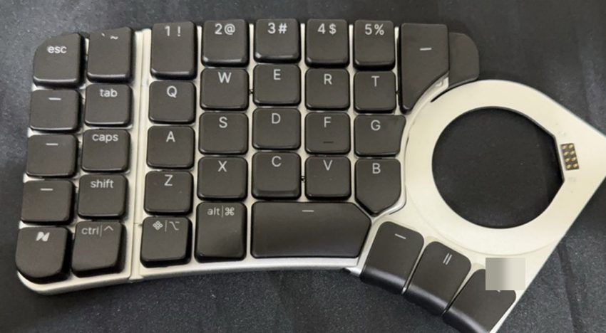
Module dock interface on the half (pogo board, contacts, bay)
Photos: left CRL IP2 p15, CRL IP1 p5, p7; right CRR IP2 p13, CRR IP1 p5-p6; exterior CRL EP p2-p4, CRR EP p2-p4.
| ID | Image | Location | Part | Maker | Function | Marking as read | Source | Basis | Notes |
|---|---|---|---|---|---|---|---|---|---|
| PD-03 | 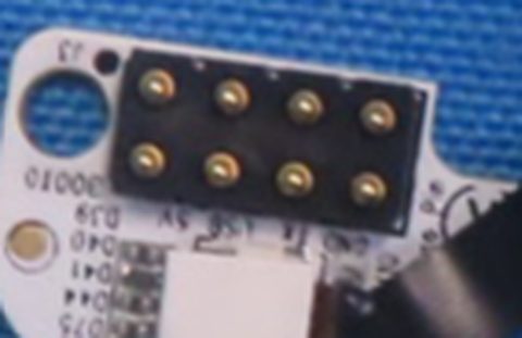 |
Pogo board contact face, on the straight chord of the bay opening (both halves) | 8-position spring (pogo) pin block, unmarked | not identified | Half-side module dock contacts; pins stand proud on the half, the modules carry the mating pads | 8 gold domed pins, 2 staggered rows of 4, black insulator, 8 through-hole joints [clear count]; no marking | CRL IP2 p15; CRL IP1 p5, p7; CRR IP2 p13; CRR IP1 p5, p6; CRL EP p2-p4; CRR EP p2-p4; CRL BLE p35; CRR BLE p35; CRR UM2 p2 | DOC; confirmed | Identical count on both halves and on every module (TUM-20, TCX-09, TKX-07). |
| PD-05 | 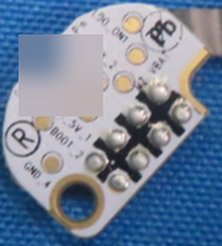 |
Pogo board pad labels | silkscreen pads | - | Same signal family as the dock board | Left back: GND_4, BOOT_2, MZ_VBAT, RX_2, …_ON1 (candidate LDO_ON1); right back: GND_4, BOOT_2, 5V_1, RX_2; right pin face: ?ND, TX, USB_5V [clear except where marked] |
CRL IP2 p15; CRR IP2 p13 | DOC; confirmed | Pin-to-signal mapping not resolvable (OQ-09). |
| PD-06 | 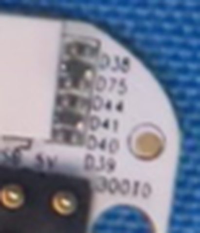 |
ESD diodes on the pogo board | small diodes, unmarked | not identified | ESD/TVS on the exposed dock lines (INFERRED) | Left: 5 parts with diode symbols (refs D19...D38); right: 6 parts (D39, D40, D41, D75, D3?); edge text ?0010 [counts clear; refs partial] |
CRL IP2 p15; CRR IP2 p13 | DOC; INFERRED (role); confirmed | - |
| PD-07 | 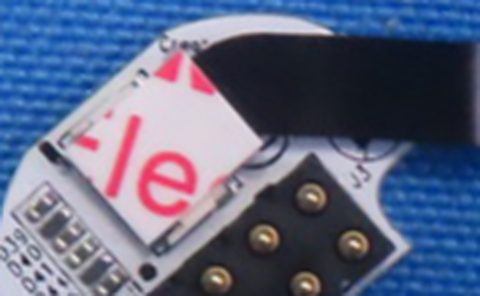 |
Pogo board connectors | flex termination / connector | - | Pogo flex termination (INFERRED) | Left: J1 under a white sticker (red text fragment le), second ref J5 or J3; right: J3 [clear] beside a round cut-out, white block at the flex exit |
CRL IP2 p15; CRR IP2 p13 | DOC; confirmed | - |
| PD-08 | 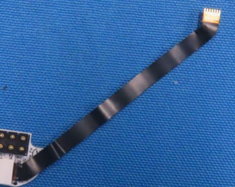 |
Pogo flex | black flat flex about 50 mm with stiffener | - | Pogo board to dock board (right: into dock J4, INFERRED) |
Right flex printed R; fingers: left about 12 (estimate), right about 7 visible [counts partial] |
CRL IP2 p15; CRL IP1 p5; CRR IP2 p13; CRR IP1 p5, p6 | DOC; INFERRED (counts, routing); confirmed | - |
| PD-09 | 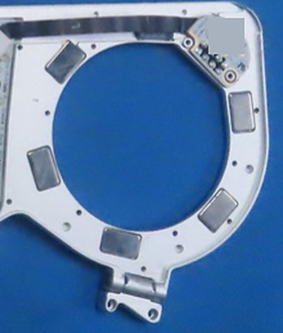 |
Module-bay bracket (both halves) | metal frame with circular opening and two hinge lugs; 5 rectangular blocks | not identified | Carries the dock and pogo boards; the 5 blocks did not attract a steel paper clip, so they are not magnets (MEASURED on one board, 2026-09-23; identity INFERRED from the test) | 5 rectangular blocks around the opening on each half [clear count] | CRL IP1 p5; CRR IP1 p5 | DOC; MEASURED (paper-clip test); confirmed | - |
| PD-10 | 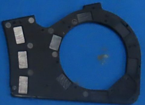 |
Magnet carrier plate under the bay bracket (left) | black plate with circular opening; at least 4 magnet-colored blocks | not identified | 4 of the 6 module-bay magnets (MEASURED: paper-clip test on one board, 2026-09-23) | 4 silver blocks like PD-09 [clear]; 6-8 darker rectangular segments of unknown material | CRL IP1 p5 | DOC; MEASURED (paper-clip test); corrected (Count narrowed from 'at least 6' to 'at least 4') | - |
| PD-11 | 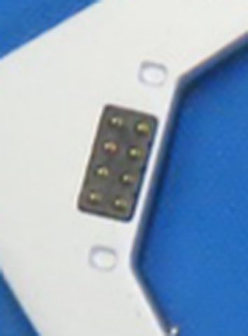 |
Two features flanking the contact block on the chord | small light oblong/round features | - | Magnets or locating features (not determinable); 2 of the 6 module-bay magnets, one on either side of the contact block (MEASURED: paper-clip test on one board, 2026-09-23) | Present on both halves [clear presence] | CRL EP p2-p4; CRR EP p2-p3; CRL BLE p35; CRR BLE p35; CRR SRD p34; CRR UM2 p2 | DOC; MEASURED (paper-clip test); confirmed | - |
| PD-12 | 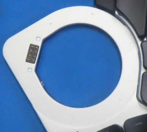 |
Dock opening in the half | circular through-cutout with one straight chord | - | Module bay: contacts on the chord; modules pressed up 'through the module dock cutout' | Small round features on the bore wall (raised or recessed, not determinable) [clear shape] | CRR EP p2, p3; CRR UM2 p2 | DOC; confirmed (Wording refined ('bumps' to 'round features')) | - |
| PD-13 | |
Dock link net set (half side and module side) | - | - | UART (TX/RX), boot select (BOOT, BOOT1), module battery rail (MZ_VBAT/VBAT), 5 V feed (USB_5V/POGOPIN_5V/5V), enable (LDO_ON/MODULE_ON/ON), GND |
Half labels HP-11, DK-10, PD-05; module labels GND, VBAT, RX, ON, GND, TX, 5V, BOOT1 (TUM-20, TCX-09, TKX-07); no D+/D- on any dock, pogo or module contact label |
CRL IP1 p9; CRL IP2 p15; CRR IP1 p12; CRR IP2 p13, p16 | DOC (labels); INFERRED (function, direction; pin order unknown); confirmed | Fits a module update driven by the half over UART plus BOOT1 (INFERRED, untested; OQ-09). |
Half enclosure, switches, keycaps, mechanics
Manual text is from user manual v1.0.6 (CRR UM1-UM5, native text layer) and the older CRL manual (image-only).
| ID | Image | Location | Part | Maker | Function | Marking as read | Source | Basis | Notes |
|---|---|---|---|---|---|---|---|---|---|
| EN-01 | 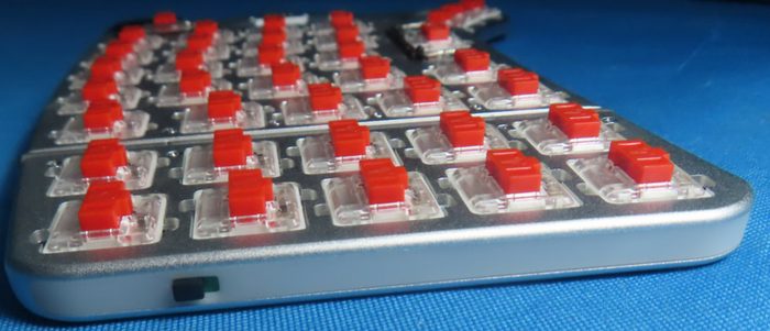 |
Key switches, 37 per half (24 body + 10 wing + 3 dock), 74 total | CPG-1232 = Kailh PG1232 ('Choc Mini'), 0.45 x 0.42 mm pin variant | Kailh (Kaihua Electronics) | Hot-swappable low-profile key switch; red stems and clear housings in the photos; PG1232 is 14.5 x 13.5 x 8.2 mm, 2.4 mm travel (Kailh) | Spec sheet 'Kailh CPG-1232 (0.45x0.42mm pin variant)' [clear, text layer]; Kailh wordmark on the manual drawing (CRR copy) |
CRR UM1 p3; CRR UM3 p2, p4; CRL UM1 p3; CRL UM2 p4, p6; CRL IP1 p5, p6; CRR IP1 p5 | DOC; confirmed | 74 keys matches NayaFlow 1.25.1's 74 key labels (STATIC). |
| EN-03 | 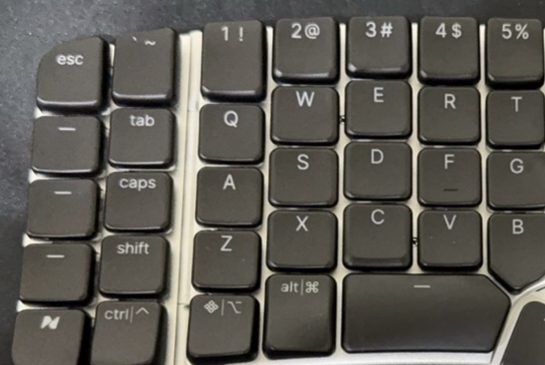 |
Keycaps, 37 per half | polycarbonate keycaps | - | Individually sculpted keycaps with a coordinate label on the underside (scheme LA1..LH4, RA1..RH4 in NayaFlow 1.25.1 geometry, STATIC) |
Spec sheet 'Keycaps: Polycarbonate' [clear]; drawing shows the underside tag as XXN |
CRR UM1 p3; CRR UM3 p2; CRL UM1 p3; CRL UM2 p4; STATIC: NayaFlow 1.25.1 key geometry | DOC; STATIC (label scheme); confirmed | - |
| EN-04 | 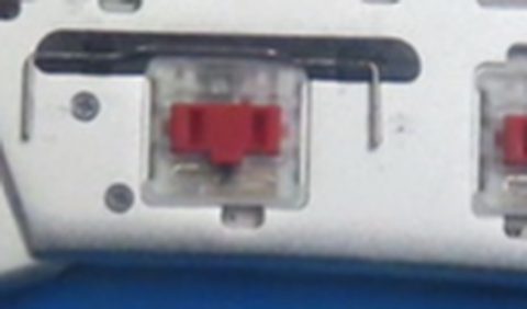 |
Stabilizers on the larger keycaps | wire-type stabilizer, unmarked | not identified | 'Larger keycaps ... have stabilizers' | Black wire bar with legs into the plate either side of one switch [clear in photo] | CRR UM3 p1, p2; CRL UM2 p3, p4; CRR IP1 p5 | DOC; confirmed | Which keys carry stabilizers is not stated. |
| EN-05 | |
Enclosure: body, dock, wing | 'Aerospace Grade Aluminum' (alloy not stated) | - | Three-section aluminum body; black dock underside plate of unknown material | Spec sheet 'Body / Dock / Wing: Aerospace Grade Aluminum' [clear] | CRR UM1 p3; CRL UM1 p3 | DOC; confirmed | - |
| EN-06 | 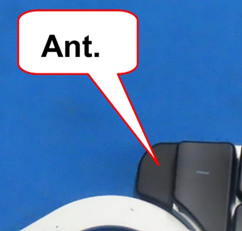 |
Black end cap at the rear-inner corner | non-metal end cap carrying USB-C | - | Antenna window behind which the RF0400A sits | Dark matte cap with USB-C; the lab's 'Ant.' callout on the top view lands on the black keycap above that corner [clear] | CRR EP p3 (vector callout), p4; CRL EP p2-p4; Kickstarter updates 14 (2024-07-24) and 15 (2024-09-03) | DOC (callout; vendor statement); confirmed | - |
| EN-07 | 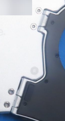 |
Hinges and tenting | wing hinge + dock hinge | - | Two tenting hinges per half, 'In-built tenting up to 27°' | Round silver pivot cap (wing); two knuckle assemblies with screws (dock) [clear] | CRR UM1 p3; CRR UM2 p1; CRL UM1 p3; CRR EP p3, p4; CRL EP p3 | DOC; confirmed | - |
| EN-08 | |
PCB suspension | foam layer (part not identified in photos) | - | 'Foam-suspended PCB for sound dampening' | Feature list text [clear] | CRR UM1 p3; CRL UM1 p3 | DOC; confirmed | - |
| EN-09 | 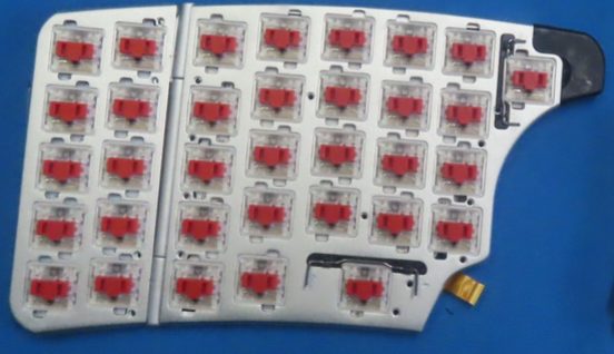 |
Switch plates | separate rigid metal plates: body (24), wing (10), dock ring (3) | - | Plates butted at seams with screws, linked only electrically by flex; the hinging is in the case (EN-07) | Plain butted seam with screws [clear] | CRR IP1 p5; CRL IP1 p5, p6 | DOC; corrected (Not 'two hinged sections') | - |
| EN-10 | 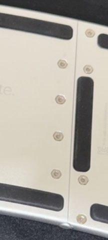 |
Underside screws | cross-recess screws | - | Fasteners: 12 silver (4 wing, 8 body) matching 12 symbols on the label outline; at least 13 small black screws around the dock ring plate | Round heads, single cross-slot [clear] | CRR EP p3, p4; CRR LBL; CRL LLOC p1 | DOC; confirmed | The count of 12 is carried from the extraction pass. The left sheet shows the same 12 screw symbols. |
| EN-11 | 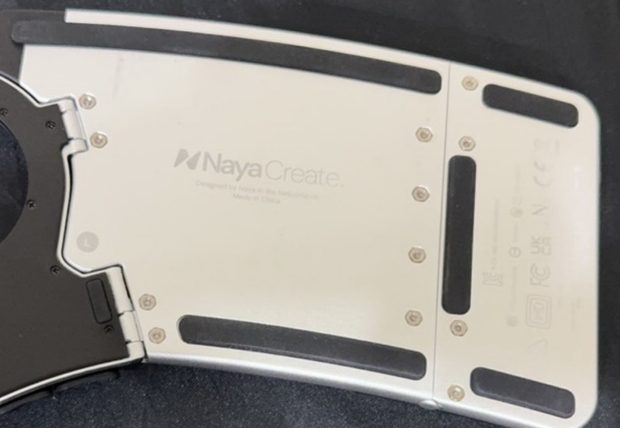 |
Feet | raised strips (rubber INFERRED) | - | Body 2 long curved strips; wing 2 short + 1 long; dock 1 long strip + 1 small pad | [clear shape] | CRR EP p3; CRR LBL; CRL LLOC p1 | DOC; INFERRED (material); confirmed | - |
| EN-12 |  |
Side marker near the lower dock hinge | L / R in a filled circle |
- | Left/right identification | R read on photo and artwork; L from the CRL photo (extraction pass) [clear] |
CRR EP p3; CRR LBL; CRL EP p2; CRL LLOC p1 | DOC; confirmed | - |
| EN-13 |  |
Underside wordmark | engraving | - | Branding and origin | 'N Naya Create.®', 'Designed by Naya in the Netherlands', 'Made in China' [clear on artwork; faint engraving] | CRR EP p3; CRR LBL; CRL LLOC p1 | DOC; confirmed | - |
| EN-14 | |
Size and weight | '212 x 118 x 18mm', '1.4kg' | - | Spec-sheet dimensions (per half INFERRED from the 1:1 label outline, about 210.3 x 121.3 mm) | Spec sheet [clear] | CRR UM1 p3; CRR LBL | DOC; INFERRED (per half); confirmed | The sheet does not say per half or per pair. |
| EN-15 | |
Half-to-half magnets | magnets (count not given) | - | 'The two halves of Naya Create are magnetically attached to one another' | Manual text [clear] | CRR UM1 p8; CRL UM1 p8 | DOC; confirmed | - |
Speedlink dongle (NAYA-100-1, board B0K17_Dongle_20241106_V01)
Photos: DG IP p4-p5 (board), DG EP p2-p3 (exterior) and the closed unit in CRR IP7 p44-p45.
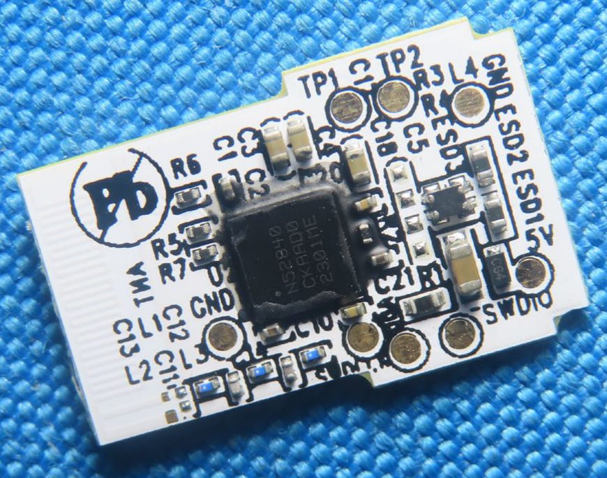
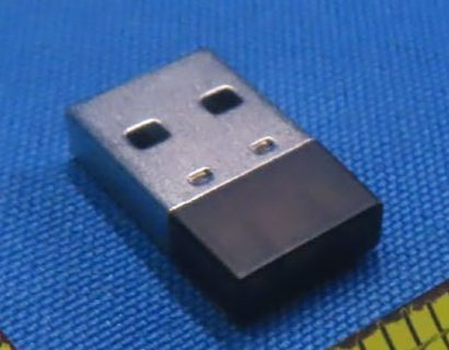
| ID | Image | Location | Part | Maker | Function | Marking as read | Source | Basis | Notes |
|---|---|---|---|---|---|---|---|---|---|
| DG-04 | 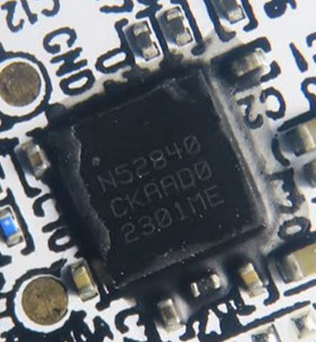 |
U1, back side |
nRF52840, package CKAA (WLCSP; about 4.0 x 3.8 mm with fillet), build code D0 | Nordic Semiconductor | BLE SoC with native USB; firmware in the internal 1 MB flash (no external flash on the board) | N52840 / CKAAD0 / 2301ME, pin-1 dot [clear] |
DG IP p5; DG RF p10-p11 (power setting 8 / 7 / 8, 8.97 dBm) | DOC; INFERRED (D0 = Revision 2); confirmed | D0 = Revision 2 (Revision 3 is Fx0), INFERRED from Nordic DevZone. |
| DG-06 | 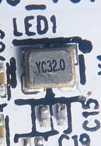 |
Y1, front |
32.000 MHz crystal, 4-pad metal lid, about 2.1 x 1.7 mm | not identified | nRF52840 HFXO | YC32.0 [clear] |
DG IP p5 | DOC; confirmed | - |
| DG-08 | 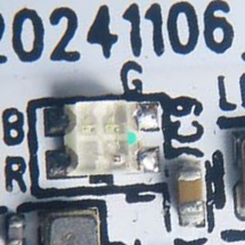 |
LED1, front |
RGB LED, 4-pad, clear lens, 3 die sites, unmarked | not identified | Status LED with a common pad | Silkscreen G, B, R at the pads [clear] |
DG IP p4, p5 | DOC; INFERRED (common pad); confirmed | MEASURED behavior: green/red during the boot identity, then white (measured on one dongle, 2026-09-11). |
| DG-09 | 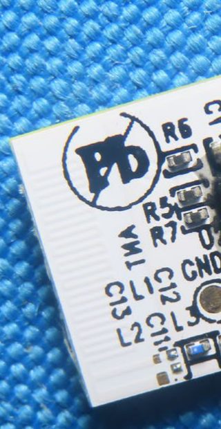 |
ANT, end opposite the USB fingers (under the plastic cap) |
RF0401A | Boen (Dongguan Boen Intelligent Technology Co., Ltd.) | 2.4 GHz PCB antenna, 10 mm long, connector N/A; filed gain 3.11 dBi = measured gain at 2480 MHz (28.18 % efficiency); 0.91-3.70 dBi and 17.8-31.6 % over 2400-2500 MHz; uncertainty 1.17 dB | Silkscreen ANT; report 'BOEN RF0401A PCB N/A 3.11' [clear] |
DG RF p10; DG OTA p1, p2, p8, p13; DG IP p5 | DOC; confirmed | OTA report BTL-OTA-1-2506C290 R00, tested 2025-07-14. The DG IP p4 'Antenna' callout arrow lands on a USB finger (probably misplaced). The SAR report's drawing puts the single antenna at the far end of the cap (DG-19). |
| DG-10 | 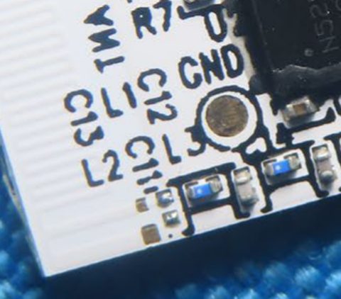 |
RF matching network | L1-L3, C11-C13, unmarked 0402 |
not identified | Pi/LC match between the SoC and the antenna (INFERRED) | Refs [clear] | DG IP p5 | DOC; INFERRED (role); confirmed | - |
| DG-11 | 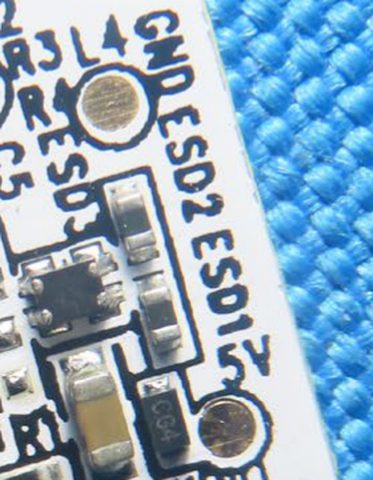 |
ESD1, ESD2 at the USB end |
2-terminal 0402 parts, unmarked | not identified | ESD on the USB lines (INFERRED) | Refs [clear] | DG IP p5 | DOC; INFERRED (role); confirmed | The adjacent 4-lead ESD3 part is U-DG-11b. |
| DG-13 | |
Passives | chip resistors and MLCCs, unmarked | not identified | Decoupling and load capacitors (C15/C16 by Y1) | R1, R3-R7; C1, C2, C3, C5, C8-C10, C15, C16, C18-C21 [mostly clear] |
DG IP p4, p5 | DOC; confirmed | - |
| DG-14 | 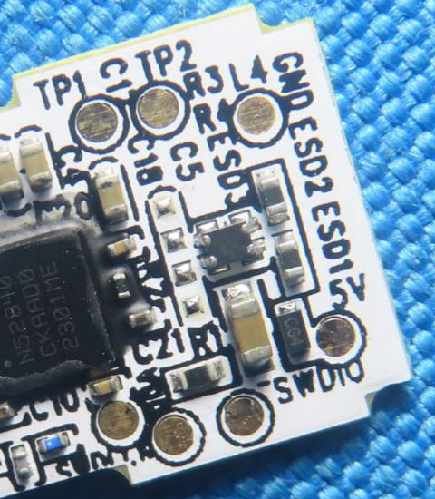 |
Test pads, back side | 8 round pads about 1 mm | - | SWD, power and test access | TP1, TP2, GND x2, 5V, SWDIO [clear]; two more cut by the board edge, fragment SW… (SWCLK expected, INFERRED) |
DG IP p5 | DOC; confirmed | - |
| DG-15 | 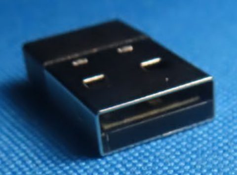 |
USB-A plug and housing | 4 gold edge fingers (USB-A pitch) in a metal USB-A shell with a dark rear cap | - | Nano-class USB-A receiver, about 20-21 mm overall, about 11 mm proud of the host (INFERRED) | Shell with latch windows; no text [clear] | DG IP p4, p5; DG OTA p1; CRR IP7 p44, p45; DG EP p2-p3 | DOC; INFERRED (sizes); confirmed | - |
| DG-16 | |
Absent parts (both faces) | none | - | No external flash, USB bridge, PA/LNA, battery or charger | Only one IC-class part (U1) on either face [clear] | DG IP p4, p5 | DOC (absence); INFERRED; confirmed | - |
| DG-18 | |
Closed dongle exterior | no product marking | - | No FCC ID, model or product text on shell or cap; only a lab sample tag on the cap (value withheld) | [clear] | CRR IP7 p44, p45; DG OTA p1; DG EP p2-p3 | DOC (absence); confirmed | The dongle filing's own exterior photos (DG EP p2-p3) show no FCC ID, model or logo anywhere, only a lab tag. |
| DG-19 | 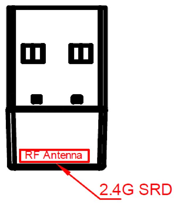 |
Antenna position | - | - | Drawing of the dongle: the plug end with two double-slot windows and two dimples, then the cap; 'RF Antenna' at the far end of the cap; 'The EUT only has one antenna and does not have synchronous transmission function' | [clear] | DG SAR p22, p27 | DOC; new (2026-09-23 exhibits) (one extraction pass, no blind re-read) | - |
Naya Tune main board (ring PCB, Tune_MB_20250227_V09)
One sample, photographed once: CRL p17-p26 = CRR p14-p23 (same JPEG files).
| ID | Image | Location | Part | Maker | Function | Marking as read | Source | Basis | Notes |
|---|---|---|---|---|---|---|---|---|---|
| TUM-03 | 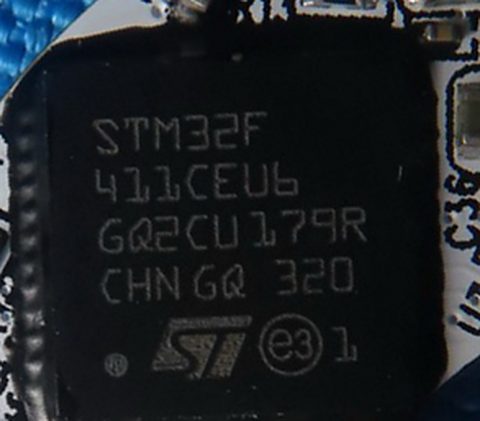 |
MCU (refdes not legible beside the chip; U1 per an earlier reading) |
STM32F411CEU6 (UFQFPN48, 7 x 7 mm) | STMicroelectronics | Module MCU: Cortex-M4F 100 MHz, 512 KB flash, 128 KB RAM, USB OTG FS | STM32F / 411CEU6 / GQ2CU179R / CHN GQ 320, ST logo, e3, 1 [clear] |
CRL IP3 p19-p20 = CRR IP2 p16-p17 | DOC; INFERRED (320 = 2023 week 20); confirmed |
- |
| TUM-04 | 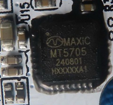 |
U15 |
MT5705 | Maxic Technology | Qi (WPC 1.2.4 BPP) 5 W wireless-power receiver SoC, QFN32 4 x 4 mm, Cortex-M0, I2C slave | MAXiC / MT5705 / 240801 / HXXXXA1 [clear; line 4 is a printed lot code] |
CRL IP3 p19-p20 = CRR IP2 p16-p17 | DOC; confirmed | QI_?X_SCL/QI_?X_SDA pads give the MCU an I2C link to it. |
| TUM-05 | 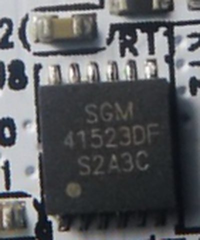 |
U8 |
SGM41523 (base variant; ordering code SGM41523YTDF12G/TR) | SG Micro | 2.5 A standalone switch-mode single-cell Li-ion charger, TDFN-3x3-12L, 1.33 MHz, no I2C, JEITA, TS/NTC input | SGM / 41523DF / S2A3C [clear] |
CRL IP3 p20-p21 = CRR IP2 p17; CRR IP3 p18 | DOC (marking matches the datasheet marking table); confirmed | - |
| TUM-06 | 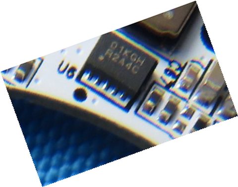 |
U6, beside an R47 inductor |
SGM62117 (SGM62117XTGH10G/TR) | SG Micro | Synchronous 4-switch buck-boost converter, 2.2-5.5 V in, 1.8-5.2 V out, 2 A, TDFN-3x2-10L | 01KGH (first glyph consistent with 0) / H2A4C or ?2A4C [line 1 clear; line 2 partial] |
CRL IP3 p19-p20 = CRR IP2 p16-p17 | DOC (datasheet marking 01KGH); INFERRED (role); confirmed (Upgraded from 'probable' to a marking match) |
Role (3.3 V rail from the cell, or 5 V toward the dock) INFERRED. |
| TUM-09 | 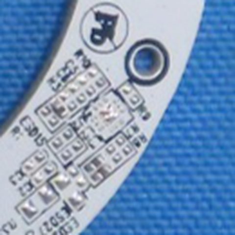 |
Unpopulated IC footprint ringed by ESD15, ESD24, ESD27, R8, R9 |
none (DNP) | - | Do-not-populate option | Empty square land [clear] | CRL IP3 p19 = CRR IP2 p16 | DOC; confirmed | - |
| TUM-10 | 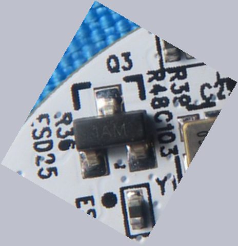 |
Q3 |
MMBT3904 class NPN, SOT-23 | multi-source | Small-signal NPN (40 V, 200 mA) | 1AM [clear] |
CRL IP3 p20 = CRR IP2 p17 | DOC (marking); INFERRED (code-to-part); confirmed | Q1/Q2 are U-TUM-10b. |
| TUM-11 | 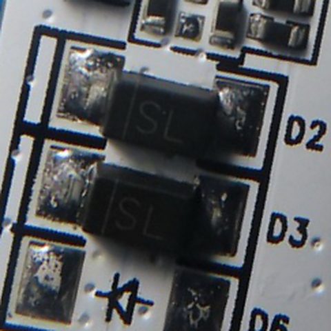 |
D2, D3 (D6 footprint unpopulated) |
B5819W class Schottky, 40 V 1 A, SOD-123 | multi-source | OR-ing of the Qi and dock inputs (INFERRED) | SL on both [clear] |
CRL IP3 p21 = CRR IP3 p18 | DOC (marking); INFERRED (code-to-part, role); confirmed | - |
| TUM-12 | 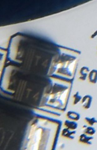 |
D4, D5 |
1N4148W class switching diode, SOD-123 | multi-source | Switching diode | T4 with cathode bar [clear in two readings] |
CRL IP3 p21 = CRR IP3 p18 | DOC; INFERRED (code-to-part); confirmed | - |
| TUM-14 | 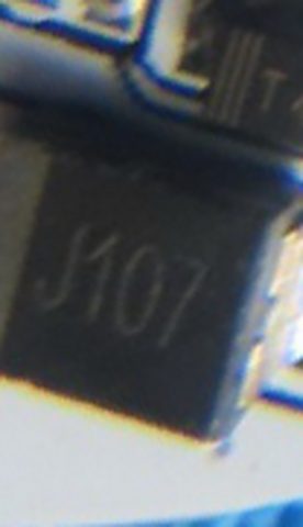 |
Polarised bulk capacitor | 100 uF tantalum/polymer (107; J is the common 6.3 V tantalum voltage code, INFERRED) |
not identified | Bulk capacitance | J107, + on the silkscreen, end band [clear after rotation] |
CRL IP3 p19, p21 = CRR IP2 p16; CRR IP3 p18 | DOC; INFERRED (voltage code); corrected (Full marking read (was ?07)) |
- |
| TUM-15 | 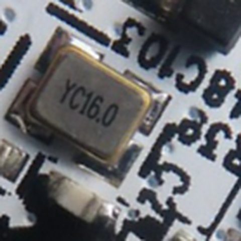 |
Y1 |
16.000 MHz crystal, 4-pad metal lid | not identified | STM32 HSE | YC16.0 [clear] |
CRL IP3 p20 = CRR IP2 p17 | DOC; confirmed | - |
| TUM-16 | 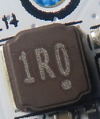 |
Inductors L14, the inductor by U6, L7, L8, L11, L13 |
1.0 uH (1R0) and 0.47 uH (R47) SMD inductors |
not identified | Charger switch-node inductor (L14, INFERRED) and the buck-boost inductor | L14 1R0 [clear]; by U6 R47 [clear, not 4R7]; other refs only |
CRL IP3 p19, p21 = CRR IP2 p16; CRR IP3 p18 | DOC; confirmed (R47 settled over the 4R7 alternative) |
- |
| TUM-17 | 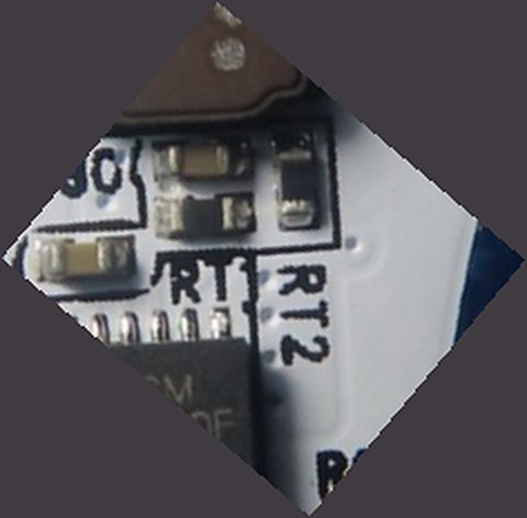 |
RT1, RT2 beside U8 |
0402 resistors | - | TS-pin divider for the pack NTC (the SGM41523 datasheet names them RT1/RT2; role INFERRED) | Refs [clear] | CRL IP3 p21 = CRR IP3 p18 | DOC; INFERRED (role); confirmed | - |
| TUM-18 | |
ESD and passives | unmarked ESD parts and passives | - | Line protection; highest refs seen: R95, C103, D40, ESD29, U15, L14, Q3, TVS1, RT2, Y1, J6 | ESD1-ESD3, ESD14, ESD15, ESD18, ESD21, ESD23-ESD27, ESD29; D1, D7, D38, D40 [clear] |
CRL IP3 p19-p21 = CRR IP2 p16-p17; CRR IP3 p18 | DOC; confirmed | - |
| TUM-19 | 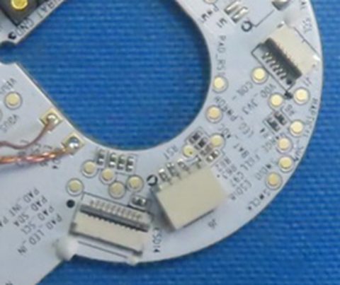 |
Board connectors | FPC and wire-to-board connectors, unmarked | not identified | FPC about 10 contacts by the PAD_* labels (to the touch disc); 2 flip-lock ZIF on the inner island; J1 small FPC about 6-8 contacts by HAPTICAL_SDA (haptic assembly, INFERRED); J6 white 4-contact header |
[clear presence; way counts are estimates] | CRL IP2 p18; CRL IP3 p19 = CRR IP2 p15-p16 | DOC; INFERRED (destinations); confirmed | Tan tape covers several connectors. |
| TUM-20 | 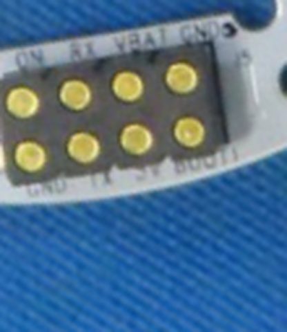 |
J5, internal dock contact block (module side) |
8-contact block, staggered 2 x 4 (1-2-2-2-1 zigzag), through-hole | not identified | Tune dock contacts | 8 gold contacts; labels GND VBAT RX ON / GND TX ?V BOOT1; two paler round pads beside the block (U-TUM-20b) [clear count] |
CRL IP2 p18; CRL IP3 p19 = CRR IP2 p15-p16 | DOC; confirmed | Corrects an earlier reading of 12 pads (2 x 6). |
| TUM-21 | 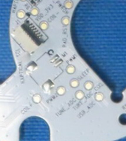 |
Actuator drive pads and footprint | pads, M1 2-pad boxed footprint |
- | Motor/coil drive (H-bridge style IN1/IN2/nSLEEP set, INFERRED), coil sensing, an I2C device inside the dial assembly | M1, PWM1 (partial), PWM2, SLEEP, COIL+, COIL-, TUNE_ADC, TUNE_ADC_COIL, HAPTICAL_SCL, HAPTICAL_SDA (partial) [clear except where marked] |
CRL IP3 p19 = CRR IP2 p16 | DOC; INFERRED (roles); confirmed | Consistent with a force-feedback dial (INFERRED). |
| TUM-22 | 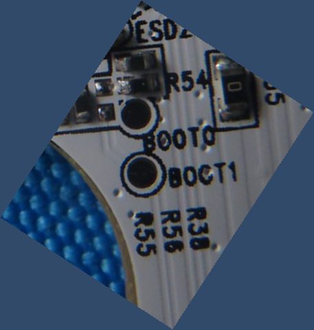 |
Debug and boot pads | test pads | - | STM32 SWD and boot straps; BOOT1 also reaches the dock block |
BOOT0, BOOT1 (beside the MCU), SWDIO, SWCL…, RST [clear to partial] |
CRL IP3 p19-p20 = CRR IP2 p16-p17 | DOC; confirmed | - |
| TUM-23 | 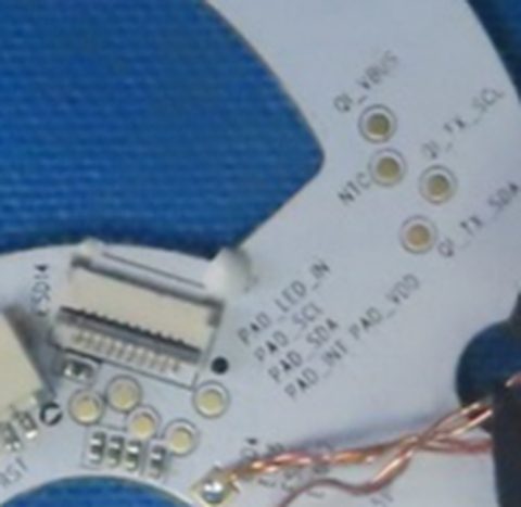 |
Other net pads | test pads | - | Touch-disc I2C + INT + RST + LED data; Qi and charger status; ADC sense | PAD_LED_IN, PAD_SCL, PAD_SDA, PAD_INT, PAD_VDD, PAD_RST; QI_VBUS, NTC, QI_?X_SCL, QI_?X_SDA; VBUS x2; USB_ADC, BAT_ADC; VDD_3V3, LED_PWRON, CHARGE_FULL [clear to partial] |
CRL IP3 p19 = CRR IP2 p16 | DOC; confirmed (Subset re-read; rest corroborated by two readings) | - |
| TUM-24 | 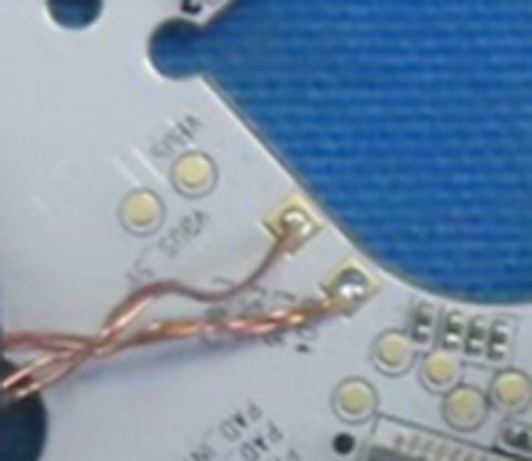 |
Qi coil landing | two square pads | - | Qi coil input (coil: TUX-18) | Twisted enamelled leads soldered on [clear] | CRL IP3 p19 = CRR IP2 p16 | DOC; confirmed | - |
Naya Tune touch/LED disc, dial, enclosure
Same shared photos as the Tune main board.
| ID | Image | Location | Part | Maker | Function | Marking as read | Source | Basis | Notes |
|---|---|---|---|---|---|---|---|---|---|
| TUX-04 | 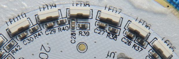 |
LED ring on the touch disc | 24 side-view RGB LEDs, white bodies, unmarked (4020 class INFERRED) | not identified | Addressable LED ring on one data line (PAD_LED_IN), no driver IC; per-LED passives C(20+n), R(31+n) |
LED1-LED24; LED1 C21 R32, LED2 C22 R33 (so C21-C44, R32-R55) [clear] |
CRL IP3 p22; CRL IP4 p23 = CRR IP3 p19-p20 | DOC; INFERRED (class); confirmed | Host side is open (OQ-08): MEASURED 2026-09-08, about 9 indices (88-96) lit with a Tune docked left; MEASURED 2026-09-19 on a donor Tune with module firmware 2.1.2, 88-93 took the host color and 94-111 stayed bright white. |
| TUX-07 | 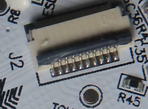 |
J2 on the disc |
10-contact flip-lock FPC receptacle, unmarked | not identified | Flex to the main board | 10 contacts (9 clear + 1 at the edge) [clear count] | CRL IP4 p23 = CRR IP3 p20 | DOC; confirmed | Corrects an earlier '~15-way' estimate. |
| TUX-08 | 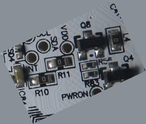 |
L4, R10, R11 on the disc |
0-ohm links | - | Jumpers | Each marked 0 [clear] |
CRL IP4 p23 = CRR IP3 p20 | DOC; confirmed | Q4/Q8 on the same board: U-TUX-08b. |
| TUX-09 | |
Disc ESD and passives | unmarked ESD parts and passives | - | Line protection around U1 | ESD1-ESD7, ESD13; R1-R11, R63 (partial); C1-C4, C83, C84 [clear] |
CRL IP4 p23 = CRR IP3 p20 | DOC; confirmed | - |
| TUX-10 | 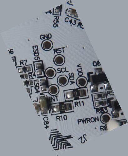 |
Disc host and power pads | test pads | - | I2C host interface (VDD, GND, SDA, SCL, RST, INT), IN, and two switched rails gated by PWRON |
VDD, GND, SDA, SCL, RST, INT, IN, PWRON, TOUCH-VDD, LED-VDD [clear; IN lower legibility] |
CRL IP4 p23 = CRR IP3 p20 | DOC; confirmed | - |
| TUX-11 | 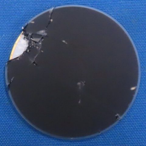 |
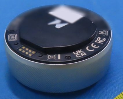
Touch cover | black glass disc about 45 mm, unmarked | - | Touch surface over the disc (marketing 'In-Built Touch Surface', INFERRED naming) | No marking; cracked edge from the teardown; about 45 mm against the tape in frame [clear] | CRL IP3 p22 = CRR IP3 p19 | DOC; confirmed | - |
| TUX-12 | 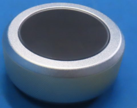 |
Dial ring | silver knurled ring, unmarked | - | Dial ring; marketed as CNC-machined aluminum, soft-knurled | No marking [clear] | CRL IP2 p17 = CRR IP2 p14 | DOC (photo; naya.tech marketing); confirmed | - |
| TUX-18 | 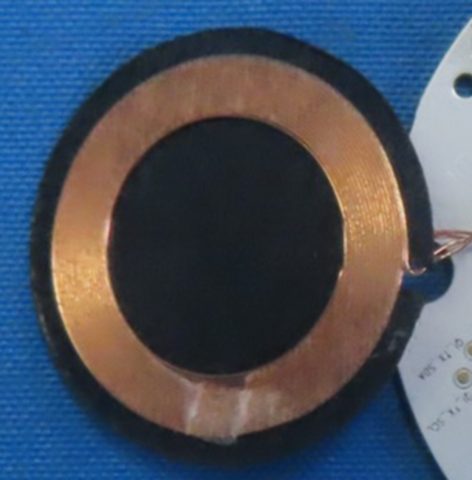 |
Qi receive coil | flat copper spiral on black ferrite, about 30-31 mm, unmarked | not identified | Qi coil feeding U15 (MT5705) | No marking; enamelled leads to TUM-24 [clear] | CRL IP2 p18; CRL IP3 p19 = CRR IP2 p15-p16 | DOC; INFERRED (size from the extraction pass); confirmed | - |
| TUX-19 | 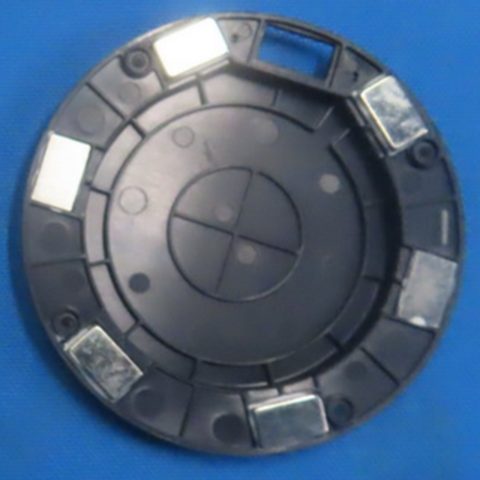 |
Base cover | black molded cover about 64 mm; 6 silver rectangular blocks; 8 flat gold pads (staggered 2 x 4) | - | Dock magnets or steel strike plates (INFERRED); module-side external dock pads | 6 blocks in rim pockets; 8 pads in a recessed block, 1-2-2-2-1 stagger [clear counts] | CRL IP2 p17-p18 = CRR IP2 p14-p15 | DOC; INFERRED (magnet vs steel); confirmed | - |
| TUX-21 | 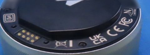 |
Base marks and fasteners | compliance marks | - | Multi-market marks on the base | CE, FCC logo, UK/CA, WEEE bin [clear]; N mark, VCI box, triangle, circle-with-bar [shape only]; at least 3-4 screws |
CRL IP2 p17 = CRR IP2 p14 | DOC; confirmed | - |
| TUX-22 | 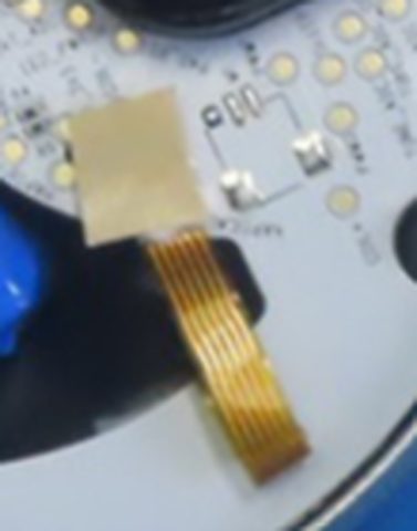 |
Internal flex | amber polyimide flex, about 7-8 traces | - | Main board to the touch/LED disc | [clear] | CRL IP2 p18 = CRR IP2 p15 | DOC; confirmed | - |
Naya Touch main board (Touch_MB_20250227_V10)
One sample: CRL p27-p36 = CRR p24-p33 (same JPEG files).
| ID | Image | Location | Part | Maker | Function | Marking as read | Source | Basis | Notes |
|---|---|---|---|---|---|---|---|---|---|
| TCM-03 | 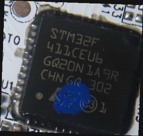 |
U1 |
STM32F411CEU6 (UFQFPN48) | STMicroelectronics | Module MCU | STM32F / 411CEU6 / GQ20N 1A9R / CHN GQ 302, ST logo, e3, 1 [clear]; 48 leads counted |
CRL IP5 p31 = CRR IP5 p28 (label-covered on CRL IP5 p29-p30 = CRR IP4 p26-p27) | DOC; confirmed | - |
| TCM-05 | 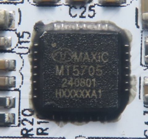 |
Qi receiver (refdes read U5 or U15) |
MT5705 | Maxic Technology | Qi 5 W receiver | MAXiC / MT5705 / 240801 / H…A1 [lines 1-3 clear; line 4 partial] |
CRL IP5 p30-p31 = CRR IP4 p27; CRR IP5 p28 | DOC; confirmed | - |
| TCM-06 | 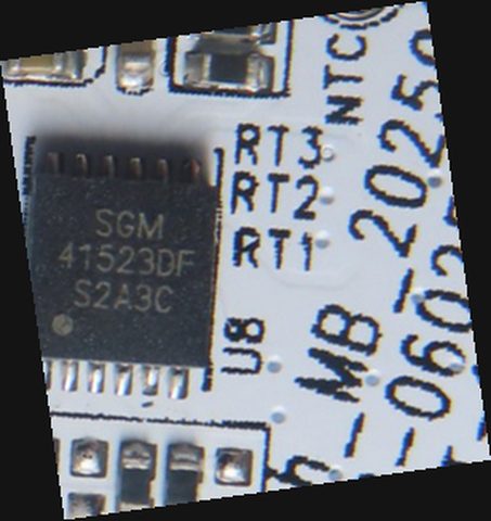 |
U8, beside R7, C18, C19, Q4, RT1-RT3 |
SGM41523 (base variant) | SG Micro | Single-cell switch-mode charger, TDFN-3x3-12L (12 leads) | SGM / 41523DF / S2A3C [clear] |
CRL IP5 p30-p31 = CRR IP4 p27; CRR IP5 p28 | DOC; confirmed | - |
| TCM-09 | 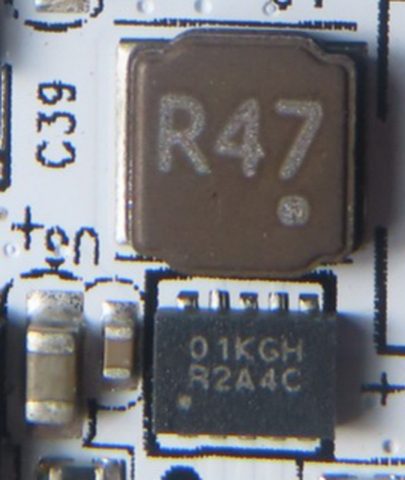 |
U3 (one reading U5), beside the R47 inductor |
SGM62117 | SG Micro | Buck-boost converter, TDFN-3x2-10L | 01KGH / R2A4C, pin-1 dot [clear] |
CRL IP5 p31 = CRR IP5 p28 | DOC (datasheet marking 01KGH); confirmed |
Role (3.3 V rail from the cell, or 5 V toward the dock) INFERRED. |
| TCM-10 | 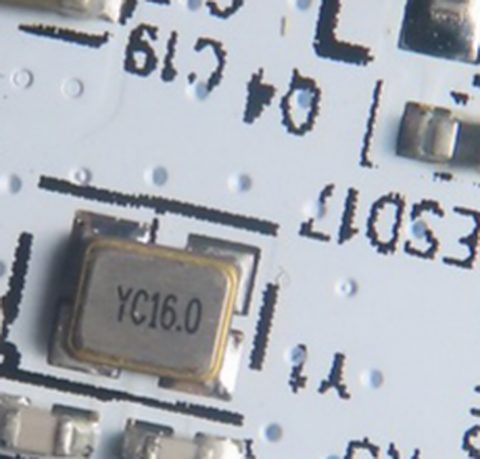 |
Y1 |
16.000 MHz crystal | not identified | STM32 HSE | YC16.0 [clear] |
CRL IP5 p31 = CRR IP5 p28 | DOC; confirmed | - |
| TCM-12 | 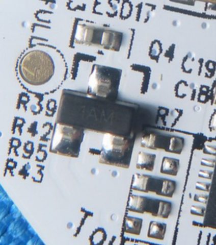 |
Q4 |
MMBT3904 class NPN, SOT-23 | multi-source | Small-signal NPN | 1AM [clear] |
CRL IP5 p31 = CRR IP5 p28 | DOC; INFERRED (code-to-part); confirmed | - |
| TCM-13 | 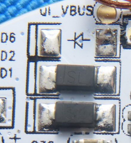 |
D1, D2 (D6 unpopulated), near QI_VBUS |
B5819W class Schottky, SOD-123FL | multi-source | Input OR-ing (INFERRED) | SL on both [clear] |
CRL IP5 p31 = CRR IP5 p28 | DOC; INFERRED; confirmed | - |
| TCM-15 | 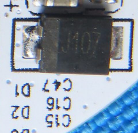 |
Probably C47, below the C47/D1 labels |
100 uF 6.3 V tantalum (EIA J = 6.3 V, 107 = 100 uF) |
not identified | Bulk capacitance | J107 [clear after 180° rotation] |
CRL IP5 p31 = CRR IP5 p28 | DOC; INFERRED (code decode); confirmed | The nearby + silkscreen belongs to an adjacent unpopulated footprint. |
| TCM-16 | 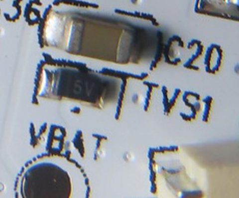 |
TVS1, beside VBAT/NTC |
5 V TVS diode | not identified | Battery-line protection (INFERRED) | 5V [clear] |
CRL IP5 p31 = CRR IP5 p28 | DOC; confirmed | - |
| TCM-17 | 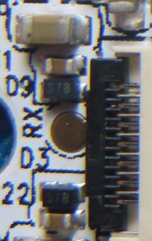 |
D3, D22; D72, D74 |
S78: not identified; T4: 1N4148W class (INFERRED) |
not identified | Small signal or protection diodes | S78 on D3 and D22 [clear]; T4 on D72 and D74 [clear] |
CRL IP5 p31 = CRR IP5 p28 | DOC; corrected (S78 settled over S7B) |
- |
| TCM-18 | 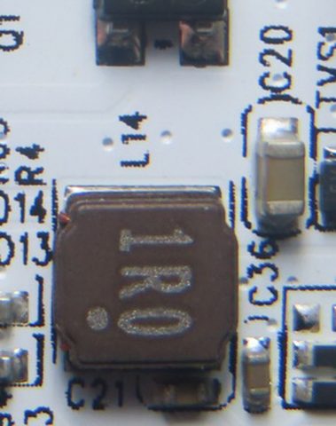 |
Inductors | 1.0 uH (1R0, L14) and 0.47 uH (R47, L2 per one reading) |
not identified | Charger inductor (INFERRED) and buck-boost inductor | 1R0, R47 [clear]; L1, L13 refs only |
CRL IP5 p30-p31 = CRR IP4 p27; CRR IP5 p28 | DOC; confirmed | - |
| TCM-19 | 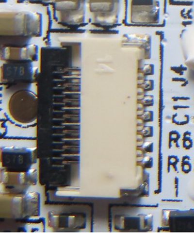 |
J4 |
14-position flip-lock FPC receptacle, about 0.3 mm pitch | not identified | Takes the pogo-board flex (TCX-11) | Molded 14 on the actuator; 13-14 contacts [clear] |
CRL IP5 p30-p31 = CRR IP4 p27; CRR IP5 p28 | DOC; INFERRED (pitch); confirmed | Corrects an earlier '~24-way' estimate. |
| TCM-20 | 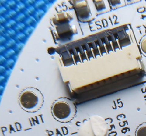 |
J5 |
8-position FPC receptacle, about 0.5 mm pitch | not identified | Takes the sensor board's 8-way J1 tail (INFERRED) |
8 contacts [clear] | CRL IP5 p30-p31 = CRR IP4 p27; CRR IP5 p28 | DOC; INFERRED (pitch, mating); confirmed | Corrects an earlier '~10-way' estimate. |
| TCM-22 | 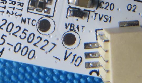 |
J3 battery header, VBAT and NTC pads beside |
3-position right-angle wire-to-board header, about 1.0 mm pitch | not identified (JST SH class not confirmed) | Battery connector (VBAT, GND, NTC INFERRED) | White housing, 3 contacts + 2 hold-down tabs; 1, 2 on the silkscreen [clear count] |
CRL IP5 p31 = CRR IP5 p28 | DOC; INFERRED (pitch, pinout); confirmed | - |
| TCM-23 | 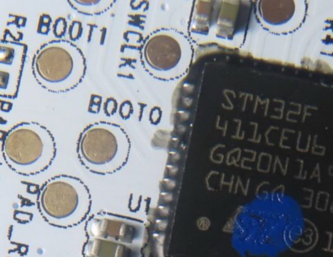 |
Debug and boot pads | test pads | - | STM32 SWD and boot straps | SWCLK1, SWDIO (partly under glue), BOOT0, BOOT1 [clear except where marked] |
CRL IP5 p30-p31 = CRR IP4 p27; CRR IP5 p28 | DOC; confirmed | - |
| TCM-24 | 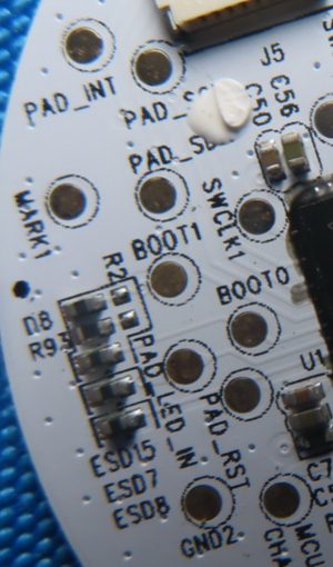 |
Other net pads | test pads | - | Sensor-board I2C, MCU-to-Qi I2C, charger status, dock insertion sense (INSERT, INFERRED), UART |
PAD_INT, PAD_RST, PAD_LED_IN, PAD_SC…, PAD_SD…, PAD_VDD, LDO_ON; QI_RX_SDA, QI_RX_SCL, QI_VBUS; MCU_3V3, VDD_3V3, USB_ADC, BAT_ADC, VBUS, VBUS_5V, CHARGE_FULL, INSERT, NTC, VBAT; TX, RX; GND2-GND4, MARK1, MARK2 [clear to partial] |
CRL IP5 p29-p31 = CRR IP4 p26-p27; CRR IP5 p28 | DOC; confirmed (Subset re-read; rest corroborated by two readings) | - |
| TCM-25 | 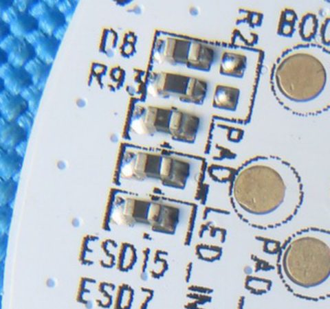 |
ESD, diodes, thermistor divider, links | unmarked parts | - | Protection; TS divider; 0-ohm links; a large DNP footprint with + |
ESD7-ESD9, ESD12-ESD15, ESD17, ESD18; D3, D8, D9, D16, D45; RT1-RT3; two parts marked 0 [clear] |
CRL IP5 p30-p31 = CRR IP4 p27; CRR IP5 p28 | DOC; confirmed | - |
Naya Touch sensor board, pogo board, enclosure
Same shared photos as the Touch main board.
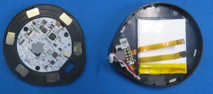
| ID | Image | Location | Part | Maker | Function | Marking as read | Source | Basis | Notes |
|---|---|---|---|---|---|---|---|---|---|
| TCX-02 | 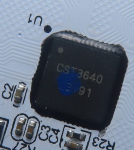 |
U1 on the sensor board |
CST3640 (QFN52 6 x 6 mm per the JLCPCB CST3640H listing, INFERRED) |
Hynitron | Capacitive multi-touch controller, I2C | CST3640 [clear] / [??]91 (1-2 characters under a blue ink dot) |
CRL IP6 p35-p36 = CRR IP5 p32-p33 | DOC (marking); INFERRED (package); confirmed | - |
| TCX-04 | 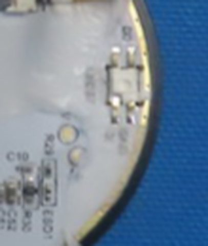 |
LED1 on the sensor board |
single addressable RGB LED, 4-pad, white body, round lens, unmarked | not identified | Module status LED (driven through the first index of its bay block) | Pad DO; R29, R30, C10, C51, C52, ESD1 nearby [clear] |
CRL IP6 p35 = CRR IP5 p32; measured on one keyboard with one Touch, 2026-09-10 (firmware not recorded with the reading) | DOC; INFERRED (class); MEASURED (a Touch lights through index 88 or 112 only, 2026-09-10); confirmed | - |
| TCX-05 | 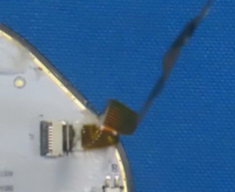 |
J1 on the sensor board |
8-contact FPC, orange 8-trace tail | not identified | Link to main-board J5 |
8 contacts, pin-1 mark [clear] | CRL IP6 p35 = CRR IP5 p32 | DOC; confirmed | - |
| TCX-06 | 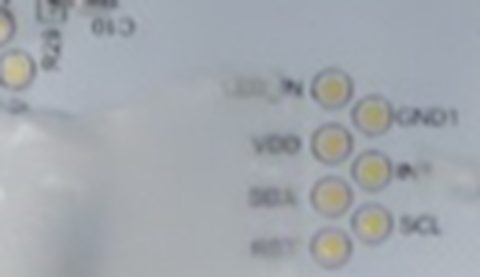 |
Sensor-board host pads | test pads | - | I2C + INT + RST + LED data | LED_IN, GND1, VDD, INT, SDA, SCL, RST [clear to partial] |
CRL IP6 p35-p36 = CRR IP5 p32-p33 | DOC; confirmed | - |
| TCX-07 | 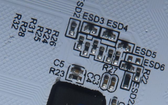 |
Sensor-board support parts | unmarked passives and ESD | - | Protection and decoupling; slotted gold pad = ground/spring land (INFERRED) | ESD2-ESD6, ESD22; R22-R28, R31, R32; C2-C5 [clear] |
CRL IP6 p35-p36 = CRR IP5 p32-p33 | DOC; confirmed | - |
| TCX-09 | 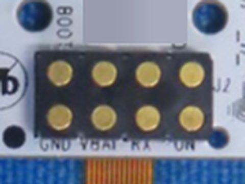 |
J2, dock contact block on the Touch pogo board |
8 gold domed contacts, 2 columns of 4, black molded block | not identified | Touch module-side dock contacts | Labels GND, VBAT, RX, up-arrow, …ON, BOO…, GND [clear count] |
CRL IP4 p28; CRL IP5 p32 = CRR IP4 p25; CRR IP5 p29 | DOC; confirmed | Corrects an earlier '2 x 5' reading. |
| TCX-10 | 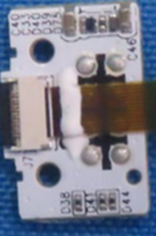 |
Touch pogo board, back | J7 FPC (about 8 contacts) and filter parts |
not identified | ESD and filtering on the dock lines | J7; C39, C40, C44, C46, D38-D41, D75; 4 joints round a cross cut-out; three small SMD parts with refs starting E on the edge [clear] |
CRL IP4 p28; CRL IP5 p32 = CRR IP4 p25; CRR IP5 p29 | DOC; corrected (Three separate SMD parts, not a stacked small board) | The round black part beside the block is U-TCX-10b. |
| TCX-11 | 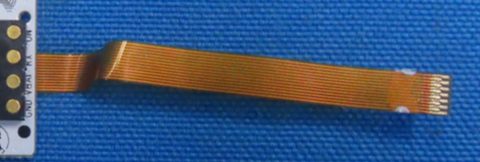 |
Touch pogo flex | amber flex about 40-42 mm, 13-14 conductors at about 0.3 mm | - | Pogo board into main-board J4 |
About 13 traces resolvable [clear] | CRL IP5 p32 = CRR IP5 p29 | DOC; INFERRED (pitch); confirmed | - |
| TCX-13 | 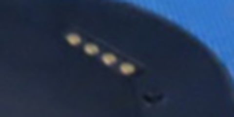 |
Touch base exposed contacts | one straight row of 4 round gold contacts in a slot | - | Exposed module-to-dock contacts | 4 contacts plus a small round feature [clear count] | CRL IP4 p27 = CRR IP4 p24 | DOC; confirmed | Relation to the 8 contacts on the pogo board is open (OQ-11). |
| TCX-14 | 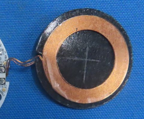 |
Qi receive coil | single-layer spiral about 29-30 mm OD, 19-20 mm ID, on a ferrite disc about 33 mm | not identified | Qi coil feeding the MT5705 | No marking; scribed cross on the ferrite [clear] | CRL IP4 p28; CRL IP5 p29-p30 = CRR IP4 p25-p27 | DOC; INFERRED (sizes); confirmed | - |
| TCX-15 | 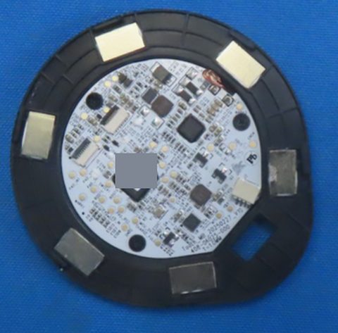 |
Carrier frame | black plastic ring with 6 silver rectangular plates and a rectangular window | - | Holds the main board; dock magnets or steel strike plates (INFERRED) | 6 plates [clear count] | CRL IP4 p28 = CRR IP4 p25 | DOC; INFERRED; confirmed | - |
| TCX-16 | 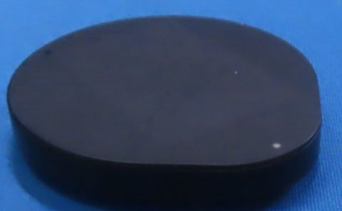 |
Top cover | glossy black teardrop cover; black glass-like disc in the teardown | - | Touch surface; small light dot near the rim = LED window (INFERRED) | No print [clear]; size unresolved (U-TCX-16b) | CRL IP4 p27; CRL IP6 p35 = CRR IP4 p24; CRR IP5 p32 | DOC; confirmed | - |
| TCX-17 | 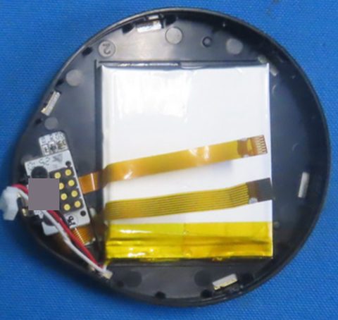 |
Housing | black shell with a molded 2 in a circular boss |
- | Enclosure; 2 is probably a mold cavity number (INFERRED) |
2 [clear]; cell held with yellow tape |
CRL IP4 p28 = CRR IP4 p25 | DOC; INFERRED; confirmed | - |
| TCX-18 | 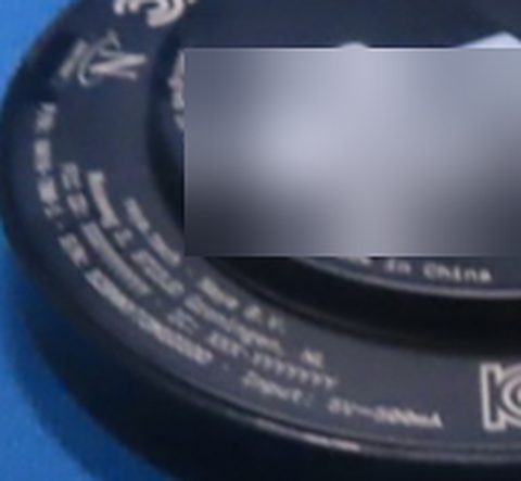 |
Touch base label | label artwork with unfilled certification placeholders | - | Printed before any module certification; no module FCC ID exists | …Netherlands · Made in China; …Naya B.V.; …, NL; XXX-YYYYYYY (IC style), R-C?-ABC-XXX… (KC style), XXX-ABC… (Japan style), 13-character CC… (NCC style); Input: 5V⎓500mA [clear to partial] |
CRL IP4 p27 = CRR IP4 p24 | DOC; INFERRED; confirmed | - |
| TCX-19 | 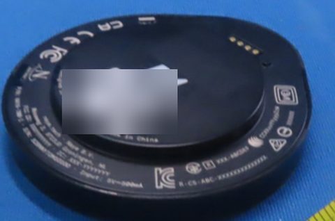 |
Touch base marks | compliance marks | - | Marks beside the placeholder text | FCC, CE, UKCA, WEEE, KC, N in an arc, RCM-like triangle, others [clear to shape only] | CRL IP4 p27 = CRR IP4 p24 | DOC; confirmed | - |
Naya Track main board (ring PCB, Track_MB_20250305_V13)
One sample: CRL p37-p46 = CRR p34-p43 (same JPEG files). IC close-ups are CRL IP7 p45-p46 = CRR IP7 p42-p43.
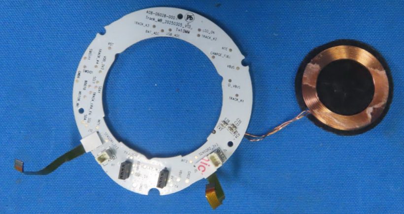
| ID | Image | Location | Part | Maker | Function | Marking as read | Source | Basis | Notes |
|---|---|---|---|---|---|---|---|---|---|
| TKM-03 | 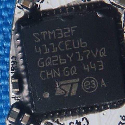 |
MCU | STM32F411CEU6 (UFQFPN48) | STMicroelectronics | Module MCU | STM32F / 411CEU6 / GQ26Y17VQ / CHN GQ 443, ST logo, e3, A [clear] |
CRL IP7 p45 = CRR IP7 p42 (under a 2D label on CRL IP7 p44 = CRR IP6 p41) | DOC; INFERRED (443 = 2024 week 43); confirmed |
- |
| TKM-05 | 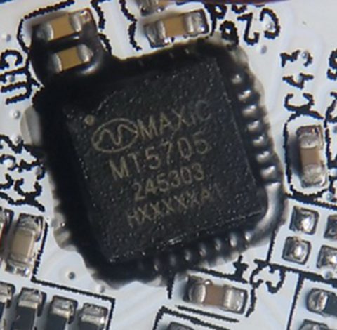 |
Qi receiver (refdes read U15 or U5) |
MT5705 | Maxic Technology | Qi 5 W receiver | MAXIC / MT5705 / 245303 / H…A [lines 1-3 clear] |
CRL IP7 p46 = CRR IP7 p43 | DOC; confirmed | Different lot (245303) from the Tune and Touch parts (240801). |
| TKM-06 | 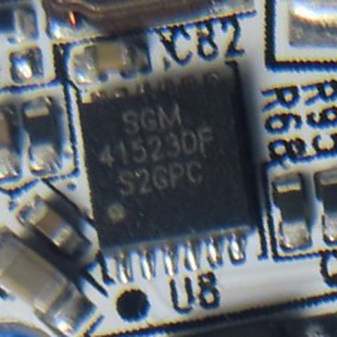 |
U8 |
SGM41523 (base variant) | SG Micro | Single-cell switch-mode charger | SGM / 41523DF / S2GPC [clear] |
CRL IP7 p46 = CRR IP7 p43 | DOC; corrected (Third line S2GPC, not S26PC) |
- |
| TKM-07 | 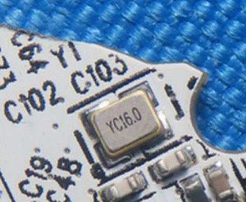 |
Y1, load caps C102, C103 |
16.000 MHz crystal | not identified | STM32 HSE | YC16.0 [clear] |
CRL IP7 p45 = CRR IP7 p42 | DOC; confirmed | - |
| TKM-11 | 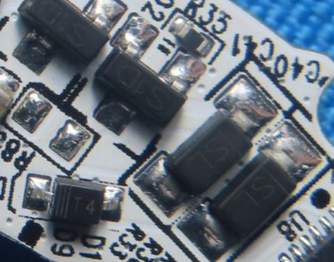 |
Two diodes near C40/C41; one near D16 |
SL: 1N5819W / B5819W class Schottky (SOD-123FL); T4: 1N4148WS class switching diode (SOD-323) |
multi-source | Schottky power-path diodes and a small-signal switching diode | SL on two parts, T4 with cathode bar on the third [clear] |
CRL IP7 p46 = CRR IP7 p43 | DOC; INFERRED (code-to-part); corrected (Two different diode families, not one class) | - |
| TKM-12 | 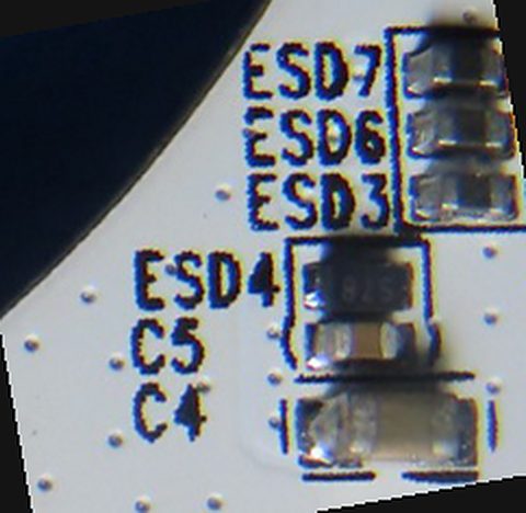 |
ESD parts | unmarked ESD/TVS parts | - | Line protection | ESD3, ESD4, ESD6, ESD7, ESD11, ESD15, ESD25 (+ ESD22, ESD27 from the extraction pass) [clear] |
CRL IP7 p45 = CRR IP7 p42; CRL IP7 p46 = CRR IP7 p43 | DOC; confirmed | The ESD4 part's own marking is U-TKM-12b. |
| TKM-13 | 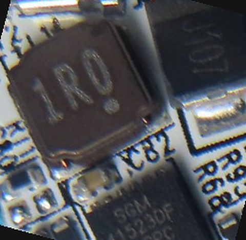 |
Inductors and links | 1.0 uH (1R0) power inductor; 0-ohm link in L13; coil pads at L11 |
not identified | Charger inductor (INFERRED); Qi coil landing | 1R0 [clear]; L13 part marked 0; second inductor 10… [partial]; L1, L11 refs |
CRL IP7 p45 = CRR IP7 p42; CRL IP7 p46 = CRR IP7 p43 | DOC; confirmed | - |
| TKM-15 | 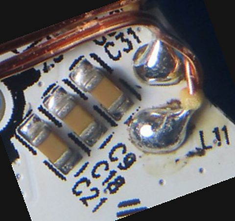 |
C9, C18, C21, C31 at the coil pads |
larger MLCCs, unmarked | - | Qi resonant/filter bank (INFERRED) | Refs [clear] | CRL IP7 p46 = CRR IP7 p43 | DOC; INFERRED (role); confirmed | - |
| TKM-16 | 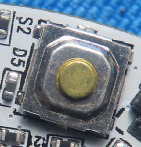 |
S2-S5 |
SMD tactile switches, metal frame, round brass actuators about 4-5 mm, unmarked | not identified | The four Track buttons (mapping to TRACK_K1-K4 INFERRED) |
S2, S4, S5 [clear], S3 [partial] |
CRL IP7 p45 = CRR IP7 p42; CRL IP7 p46 = CRR IP7 p43; CRR IP6 p41; measured on one Track, 2026-09-06 | DOC; MEASURED (four buttons, bitmask 1/2/4/8, 2026-09-06); confirmed | - |
| TKM-17 | 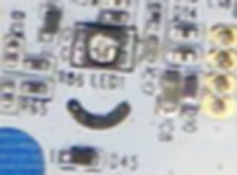 |
LED1 between the two 1x4 pad rows |
square top-view LED with round lens, unmarked | not identified | The Track's single status LED (RGB per marketing, INFERRED) | LED1 [clear] |
CRL IP7 p45 = CRR IP7 p42 | DOC; confirmed | One LED on the board supports the 'single dot' reading over the '~15 LEDs' band-pass note (OQ-08). |
| TKM-18 | 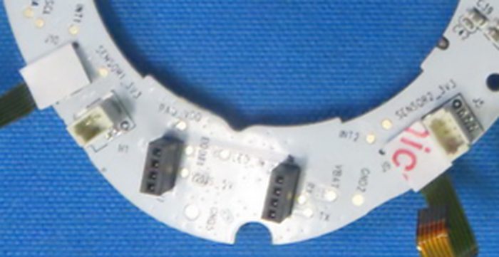 |
Connectors | wire-to-board and board-to-board sockets, unmarked | not identified | M1 white 2-way (motor) by SENSOR1_3V3; white 4-way under red-printed tape by SENSOR2…; two black 4-position female sockets by GND2/VBAT/RX/TX/?AD_VDD (take the interposer, INFERRED) |
[clear presence] | CRL IP7 p44 = CRR IP6 p41 | DOC; INFERRED (roles); confirmed | - |
| TKM-19 | 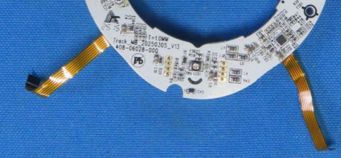 |
FPC tails | two orange FPC tails soldered to the ring | - | To the two sensor boards (INFERRED) | About 5-8 and 9-10 conductors [counts estimated] | CRL IP7 p44 = CRR IP6 p41 | DOC; confirmed | - |
| TKM-20 | 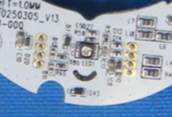 |
Pad rows either side of LED1; extra pad clusters near R22/R23/R26/R27 |
two 1x4 rows of bare plated through-holes | - | Programming header, board attach or DNP option (unknown) | Pad rows unpopulated [clear]; 2x2 and 2-pad clusters, fitted or DNP not provable | CRR IP7 p42, p43 | DOC; confirmed | - |
| TKM-21 | 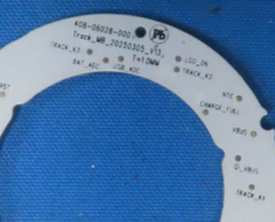 |
Net pads | test pads | - | Buttons, charger, SWD/boot, two sensor buses, haptic enable, dock UART | TRACK_K1-TRACK_K4; VBUS, QI_VBUS, NTC, CHARGE_FULL, LDO_ON, BAT_ADC, USB_ADC, VBAT, VDD_3V3; SWCLK1, SWDIO1, BOOT0, BOOT?, RST; SENSOR1_3V3, INT1, SCL, SDA, SCL1, SDA1, SENSOR2_3V3, INT2; TRACK_?RA_EN, MOTOR_IN?; RX, TX, USB_5V, PAD_VDD, LED_?, GND2, GND5, GND6 [clear to partial] |
CRL IP7 p44 = CRR IP6 p41 | DOC; confirmed (Subset re-read; rest corroborated by two readings) | - |
Naya Track sensor boards, pogo board, interposer, motor, enclosure
Same shared photos as the Track main board.
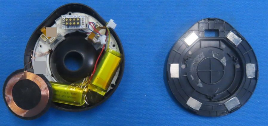
| ID | Image | Location | Part | Maker | Function | Marking as read | Source | Basis | Notes |
|---|---|---|---|---|---|---|---|---|---|
| TKX-04 | 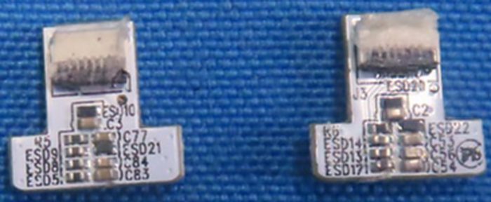 |
Sensor-board pads and parts | pads, FPC J3, ESD and passives |
- | PixArt-style 3-wire optical-sensor port (SCLK/SDIO/MOTION, INFERRED); two sensors on the ball allow twist sensing (INFERRED) |
SensorL: 3V3_SENSOR (partial), MOTION, SDIO (partial), SCLK, GND1, R11, C27, C28; SensorR: MOTION, SCLK3, SDIO3, 3V3, GND, R9; backs: J3 (about 6 contacts), ESD5, ESD8-ESD10, ESD13, ESD14, ESD17, ESD21, ESD22, C2, C3, C53-C56, C77, C83, C84, R5, R6 [clear except where marked] |
CRL IP6 p39 = CRR IP6 p36 | DOC; INFERRED; confirmed | The sensor ICs themselves are U-TKX-03. |
| TKX-07 | 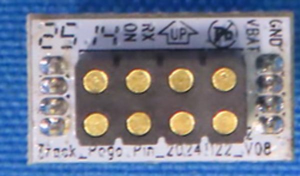 |
Track dock contacts on the pogo board | 8 gold domed contacts, 2 x 4, one black housing | not identified | Track module-side dock contacts | Labels GND, VBAT, up-arrow, RX, ON; 4 plated holes on each short edge; pitch about 2.5-3 mm (INFERRED) [clear count] |
CRL IP6 p37, p40 = CRR IP5 p34; CRR IP6 p37 | DOC; INFERRED (pitch); confirmed | Corrects an earlier '2 x 5' reading. |
| TKX-10 | 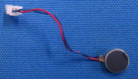 |
Haptic motor | flat coin vibration motor about 7-9 mm, unmarked | not identified | Track haptics; ERM vs coin LRA unresolved (U-TKX-10b) | Red and blue leads about 5 cm to a white 2-pin plug (mates M1) [clear] |
CRL IP6 p41 = CRR IP6 p38 | DOC; INFERRED (size); confirmed | - |
| TKX-11 | 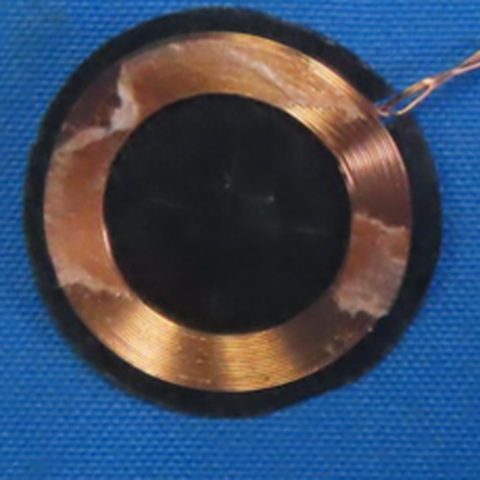 |
Qi receive coil | multi-strand spiral on black ferrite, disc about 34-35 mm (winding about 28 mm OD / 19 mm ID), foam ring | not identified | Qi coil feeding the MT5705; leads soldered at pads by L11 |
No marking [clear] | CRL IP6 p38; CRL IP7 p44, p46 = CRR IP6 p35, p41; CRR IP7 p43 | DOC; INFERRED (sizes); confirmed | - |
| TKX-12 | 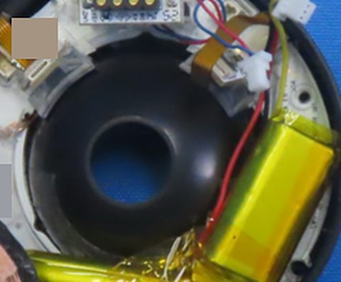 |
Ball cup and carrier | black hemispherical cup with a central hole; translucent carrier with two sensor mounts | - | Trackball socket and sensor-board carrier | Bearings not resolvable [clear shape] | CRL IP6 p38 = CRR IP6 p35 | DOC; confirmed | - |
| TKX-13 | 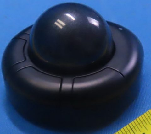 |
Trackball assembly | dark ball in a segmented top ring | - | Marketed 40 mm ball with 4 buttons; small dot at rear right = LED window (INFERRED) | Ring opening about 40 mm against the tape (INFERRED) [clear shape] | CRL IP6 p37 = CRR IP5 p34; naya.tech marketing (40 mm ball, 4 buttons) | DOC; INFERRED; confirmed | - |
| TKX-14 | 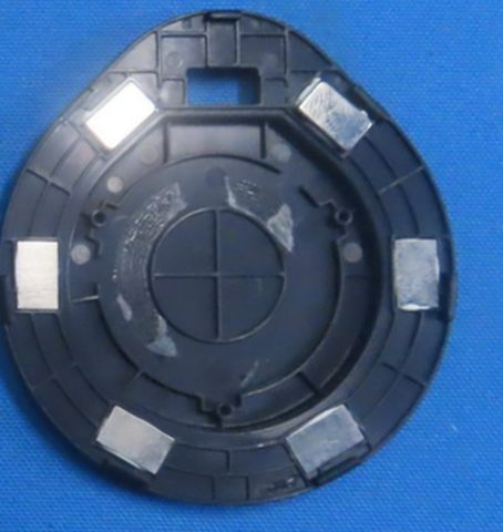 |
Base cover | black teardrop cover with 6 rectangular metal inserts, a window for the pogo block and a round seat (Qi, INFERRED) | - | Dock magnets or steel strike plates (INFERRED) | 6 inserts [clear count] | CRL IP6 p38 = CRR IP6 p35 | DOC; INFERRED; confirmed | - |
| TKX-15 |  |
Track base label | label artwork | - | Base label printed with empty certification fields | Designed in the Netherlands; naya.tech · Naya B.V.; address line; FCC ID: and IC: printed with no value [clear]; P/N: NAYA- + 2 unclear characters + 00-2 (U-TKX-15b); S/N: (withheld); Input: 5V⎓500mA [partial] |
CRL IP6 p37 = CRR IP5 p34 | DOC; confirmed (Only the P/N digits are unverifiable) | - |
| TKX-16 | 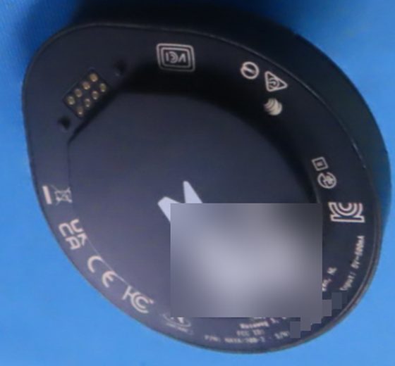 |
Track base marks and contacts | compliance marks; 8 exposed contacts | - | Marks and the exposed dock contacts | KC, CE, UK/CA, WEEE, VCCI (double box, in full), N-in-ellipse (issuer unidentified) [clear]; two marks shape-only (Giteki?, RCM?); 8 gold contacts 2 x 4 in a recess with two flanking round features |
CRL IP6 p37 = CRR IP5 p34 | DOC; confirmed | - |
| TKX-17 | 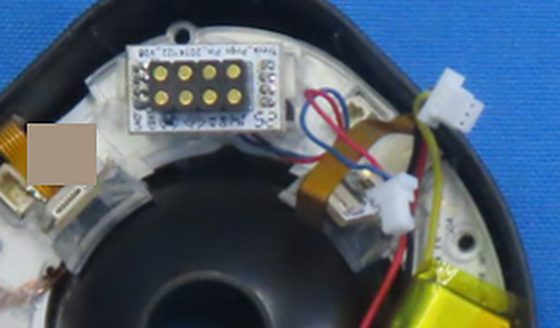 |
Internal harness | wire-to-board harness and FPC | - | White 3-pin connector (red, black, yellow-green wires; battery, INFERRED); red/blue pair to a white 2-pin plug (motor); orange FPC about 6-8 traces into a white connector | [clear presence] | CRL IP6 p38 = CRR IP6 p35 | DOC; INFERRED (roles); confirmed | - |
Batteries and power ratings (every half and every module)
Cell labels read from photos; declared values from the test reports' EUT tables.
| ID | Image | Location | Part | Maker | Function | Marking as read | Source | Basis | Notes |
|---|---|---|---|---|---|---|---|---|---|
| BAT-01 | 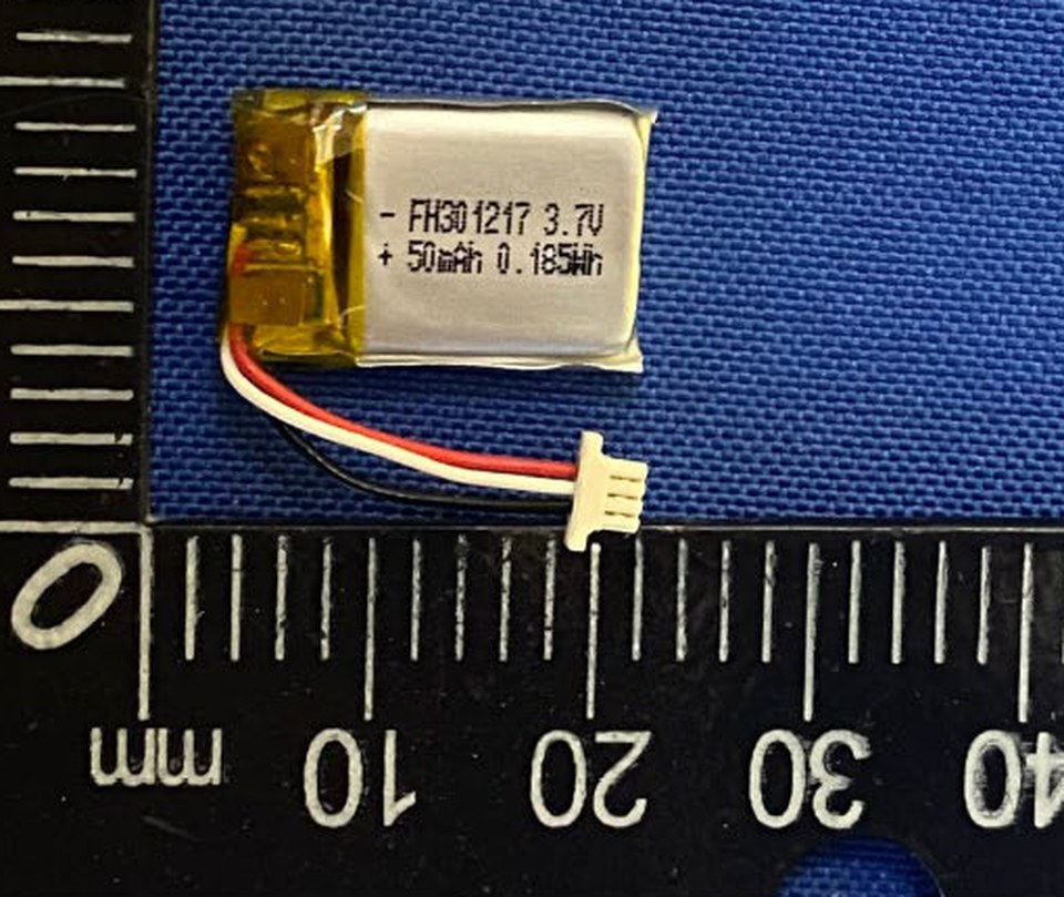 |
Each keyboard half, one cell, taped with its protection board | FH301217 (report: 'Model: 301217') |
not identified (FH prefix) |
Half cell: keeps the half on while a module is swapped; charged while the half draws power; Li-ion polymer pouch about 3.0 x 12 x 17 mm by size code (INFERRED) | - FH301217 3.7V / + 50mAh 0.185Wh [clear]; report 'Power Source 1# Supplied from battery. Model: 301217', 'DC 3.7V 50mAh 0.185Wh'; '2# Supplied from PC USB port', 'DC 5V' |
CRL IP2 p13, p14; CRL IP1 p7; CRR IP1 p10, p11; CRL BLE p10; CRL SRD p10; CRR BLE p10; CRR SRD p10; CRR UM1 p4 | DOC; INFERRED (chemistry, size); confirmed | Manual v1.0.6 spec sheet says 'Internal Battery Capacity 45mA'; the cell and the report say 50 mAh (45 is a typo or a minimum, INFERRED). |
| BAT-02 | |
Half cell lead | 3-wire lead into a white multi-contact plug (JST SH class pitch, about 1.0-1.25 mm) | not identified | Cell connection; the white wire is an NTC or ID line (INFERRED) | Red / white / black wires; 3-4 gold blades visible in the shell [clear] | CRL IP2 p14; CRR IP1 p10, p11 | DOC; INFERRED (pitch, role); confirmed | The mainboard receptacle's pin count is unresolved (U-HP-10). |
| BAT-06 | 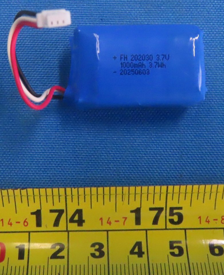 |
Naya Tune pack | FH 202030 |
not identified (FH prefix) |
Tune battery: 3.7 V 1000 mAh 3.7 Wh Li-ion polymer block pack, blue PVC wrap; about 20 x 20 x 30 mm by size code (INFERRED); 3 wires red/white/black to a white 3-position plug | + FH 202030 3.7V / 1000mAh 3.7Wh / - 20250603 [clear] |
CRL IP2 p18; CRL IP4 p25-p26 = CRR IP2 p15; CRR IP4 p22-p23 | DOC; INFERRED (size); confirmed | - |
| BAT-09 | 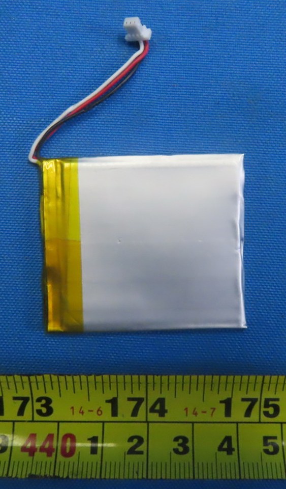 |
Naya Touch cell A | FH364046 |
not identified (FH prefix) |
Touch battery: 3.7 V 700 mAh 2.59 Wh Li-ion polymer pouch about 3.6 x 40 x 46 mm by size code (INFERRED); 3 wires red/black/white to a white 3-position plug (mates J3); protection board under yellow Kapton |
- FH364046 3.7V / 700mAh 2.59Wh / + 20250611 [clear] |
CRL IP5 p33-p34 = CRR IP5 p30-p31 | DOC; INFERRED (size); confirmed | - |
| BAT-10 | |
Naya Touch cell B (teardown layout photo) | FH364045 |
not identified (FH prefix) |
A second 700 mAh cell of the same family | - FH364045 3.7V / 700mAh 2.59WH / + 20241201 [clear; last model digit 5 on both copies] |
CRL IP4 p28 = CRR IP4 p25 | DOC; confirmed (Model digit now read (was FH36404?)) |
Whether a Touch holds one cell or two is open (OQ-20). |
| BAT-13 | 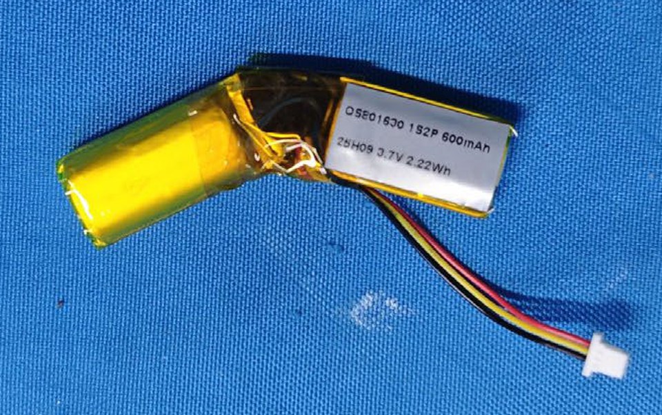 |
Naya Track pack | QS801630 1S2P |
not identified (QS prefix) |
Track battery: 3.7 V 600 mAh 2.22 Wh, two cells in parallel bent around the ring, yellow polyimide tape, nickel tabs; 3 wires red/yellow/black to a white 3-way plug | QS801630 1S2P 600mAh / 3.7V 2.22Wh; date codes 25H09 (lab photo) and 25G24 (a second, supplier-style photo) [clear] |
CRL IP6 p38; CRL IP7 p42-p43 = CRR IP6 p35, p39-p40 | DOC; INFERRED (two packs photographed); confirmed | - |
| BAT-14 | 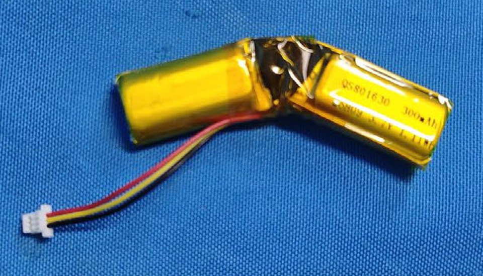 |
Naya Track cell (inside the 1S2P pack) | QS801630 single cell |
not identified | One of the two pouch cells: 300 mAh, 1.11 Wh; about 8.0 x 16 x 30 mm by size code (INFERRED); 2 x 300 mAh = 600 mAh, 2 x 1.11 Wh = 2.22 Wh | QS801630 / 300mAh / …09 3.7V 1.11Wh [partial] |
CRL IP7 p42 = CRR IP6 p39 | DOC; INFERRED (size); confirmed | - |
| BAT-16 | - | Advertised vs filed capacities | - | - | Vendor capacity figures disagree three ways (Tune / Touch / Track): website and 2023 campaign spec sheet 1500 / 800 / 800 mAh; v1.1.0 manuals 1500 / 1500 / 700 mAh; filed pre-production samples 1000 / 700 / 600 mAh | n/a | vendor website (archived); Kickstarter campaign Specs Sheet (2023); Tune, Touch and Track manuals v1.1.0 p2; BAT-06, BAT-09, BAT-13 | DOC; confirmed | Retail capacities are not confirmed (OQ-21). |
| BAT-18 | |
Module input rating (Touch and Track bases) | Input: 5V⎓500mA |
- | Module DC input rating | [clear on the Track base; clear to partial on the Touch base] | Track: CRL IP6 p37 = CRR IP5 p34; Touch: CRL IP4 p27 = CRR IP4 p24 | DOC; confirmed | - |
| BAT-19 | - | Module power path | - | - | Dock 5 V (VBUS/VBUS_5V/USB_5V) or Qi (QI_VBUS from the MT5705) through SL Schottky diodes into the SGM41523 (charger only) and the pack; power back to the half only via the VBAT dock line or a boost (SGM62117 on the Tune and Touch) |
Manual: halves' cells 'charged automatically while the keyboard is drawing power'; 'Docked modules will be charged ... if the keyboard is connected to a power source'; Qi 'both when docked and when not' [clear] | CRR UM1 p4; TUM-05, TUM-06, TUM-11, TCM-06, TCM-09, TKM-06 | DOC (parts, pads, manual); INFERRED (topology); confirmed | - |
| BAT-20 | |
Dongle power | - | - | Bus-powered; no battery, no cell in the photos | 'Power Source: Supplied from USB port', 'Power Rating: DC 5V' [clear]; label Rating: 5V⎓30mA [clear] |
DG RF p10; DG IP p4, p5; DG LBL | DOC; confirmed | - |
Accessories in the box
Box list from user manual v1.0.6 (CRR UM1 p2, native text).
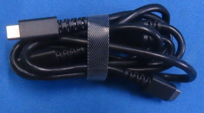
| ID | Image | Location | Part | Maker | Function | Marking as read | Source | Basis | Notes |
|---|---|---|---|---|---|---|---|---|---|
| ACC-01 | 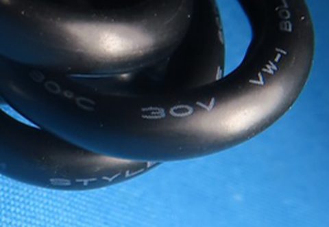 |
Box item D | '1m USB Type-C Y-Cable' | not identified | Two short USB-C ends to the halves, long USB-C end to the computer; molded splitter (no print); gray hook-and-loop strap; UL AWM class jacket (30V/80°C/VW-1 triple, INFERRED) | Jacket print 30V, VW-1 [clear], ?0°C (80 likely), STYL… (style number not legible) [partial] |
CRR UM1 p2, p6; CRL IP7 p47-p48 = CRR IP7 p46-p47 | DOC; INFERRED; confirmed | - |
| ACC-02 | - | Lab support cable | 'USB Cable, Shielded NO, Ferrite Core NO, 0.8m' | - | Cable between the EUT and the host notebook during tests; the setup photos show a Y-splitter body like ACC-01 | Support-unit table text [clear] | CRL BLE p14; CRR BLE p14, p35; CRR SRD p13, p34 | DOC; confirmed | 0.8 m (lab) vs 1 m (retail) unresolved. The CRL setup photos repeat the report photos byte for byte. |
| ACC-03 | |
Box item C | 'Speedlink Dongle' (NAYA-100-1) |
Naya | USB dongle; spec sheet 'Speedlink Connection: Using Bluetooth v5.4' | Box list; subtitle 'Wireless dongle · NAYA-100-1(Dongle)' in the CRR v1.0.6 copy only [clear] | CRR UM1 p2, p3; CRL UM1 p2 | DOC; confirmed | The dongle filing's manual is this same v1.0.6 manual: no dongle pairing procedure or LED description, one troubleshooting line ('Ensure the speedlink dongle is properly seated', UM4 p2). |
| ACC-04 | - | Box item A | 'Travel Case' | - | Clamshell case; 'can be stored in your travel case with modules attached' | [clear] | CRR UM1 p2; CRR UM2 p3 | DOC; confirmed | - |
| ACC-05 | - | Box item E | 'Keycap/Switch Puller' | - | One tool: wire keycap end, two-prong switch end | [clear] | CRR UM1 p2; CRR UM3 p1, p3 | DOC; confirmed | - |
| ACC-06 | |
Box item F | 'Spare/Sample Switches (3x)' (Kailh CPG-1232 per the spec sheet) | Kailh | Spare switches | [clear] | CRR UM1 p2, p3 | DOC; confirmed | - |
| ACC-07 | - | Box item G | 'Module Spacers (2x)' | - | Ring-shaped spacers that 'pack empty space and prevent shifting while stored' | [clear] | CRR UM1 p2; CRR UM2 p3 | DOC; confirmed | - |
| ACC-08 | 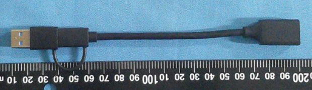 |
SAR test cable (lab, not in the box) | 'USB extension cable', 18.8 cm | - | USB-A plug on a tethered adapter sleeve at the host end, receptacle at the dongle end; used for three of the five SAR positions | [clear] | DG SAR p24; DG SAR-D photos 2, 3, 5 | DOC; INFERRED (connector reading); new (2026-09-23 exhibits) (one extraction pass, no blind re-read) | - |
Unconfirmed readings
Legible text whose identity is not established. The Candidate column is reasoning, never a part number DOC INFERRED.
| ID | Board | Location | Legible | Candidate (not a part number) | Why unconfirmed | Source |
|---|---|---|---|---|---|---|
| U-LB-11b | Identifiers | Energy mark and Japanese certification body | N crossed by an ellipse + 'ENERGY VERIFIED'; Giteki body code 219 |
- | Issuers not identified by any search | CRR LBL |
| U-HM-08 | Half mainboard | Y2, both halves |
Y2 (left), ?2 (right); 2-pad package; lid marking illegible |
32.768 kHz LFXO (INFERRED, nRF52 reference design) | Body marking out of frame or unmarked in every photo | CRL IP1 p7, p10; CRR IP1 p8 |
| U-HM-09b | Half mainboard | U1 flash, lines 2-4 (right half) |
Extraction pass: Q3??V???Q / 2?0? 6?34 (best 2208 6134) / ?0100??; adversarial re-crop: line 2 has a Q, a digit and a V, nothing assignable |
Winbond W25Q-series part (INFERRED) | Too few pixels per glyph | CRR IP1 p8 |
| U-HM-10 | Half mainboard | QSPI flash capacity | No density digit legible | 8 MB class (an earlier note, no photographic support) or 32 Mbit (if line 2 is Q3); STATIC: NayaCore 6.11.0 carries per-half images for flash generations A and B (kb_fwl.bin / kb_fwl_64.bin) chosen by PID bit 0x1000, so two capacities may exist; our units are generation A (MEASURED, keyboard firmware 3.41.0) |
The 8 MB figure has no photographic support; the Q3 read is not confirmed |
CRR IP1 p8; STATIC: NayaCore 6.11.0 (per-generation image pair kb_fwl.bin / kb_fwl_64.bin, PID bit 0x1000) |
| U-HM-13b | Half mainboard | USB-C receptacle pin class | About 13 legs counted in a partial crop | 16-pin USB 2.0 receptacle (INFERRED: the nRF52840 is USB 2.0 FS only) | Full leg row not in any crop | CRR IP1 p8 |
| U-HM-15b | Half mainboard | BOOT pad label (left) |
BOOT clear; a following 1 may belong to adjacent silkscreen |
BOOT1 |
Ambiguous glyph ownership | CRL IP1 p9 |
| U-HP-01b | Half mainboard | IC beside L11 (left) |
4-6 pad black package, pin-1 dot, no glyphs | DC-DC converter (INFERRED from the paired inductor) | No marking resolvable | CRL IP1 p9 |
| U-HP-02b | Half mainboard | U10 (left) |
6-lead SOT-23-6 package, no glyphs | Regulator or load switch (INFERRED) | No marking resolvable | CRL IP1 p9 |
| U-HP-03 | Half mainboard | QFN/DFN between R78, R79, R80, C101 (left) |
Black square package; leads sub-pixel; no marking | Battery charger or power manager (INFERRED from nearby USB_ADC, BAT_ADC, VBUS_5V, CHG_?NT) |
No marking resolvable | CRL IP1 p9 |
| U-HP-04 | Half mainboard | 2-terminal part beside R79 (C110, C32) (left) |
Uniform black molded body, no band, no code | Schottky diode (INFERRED from shape) | No marking | CRL IP1 p9 |
| U-HP-06 | Half mainboard | Epoxy glob beside R90, R13, R89, R87 (left) |
Irregular black potting, no leads or marking | - | Covered | CRL IP1 p9 |
| U-HP-07 | Half mainboard | Q1, Q6, Q8-Q11 (left); Q1 (right) |
Left: SOT-23 bodies, markings illegible (Q7 empty); right Q1: S2U (middle glyph 2 or Z) |
Load switches for the module, LED and 5 V rails (INFERRED) | S2U has no entry in the marking-code databases reached (s-manuals.com S2, 2U); search-engine summaries gave two contradictory identities |
CRL IP1 p9; CRR IP1 p8 |
| U-HP-08 | Half mainboard | Small package near C101/R12 (right) |
3-5 leads; refdes U3 or U5; marking illegible |
Small regulator or logic part (INFERRED) | No marking resolvable | CRR IP1 p8 |
| U-HP-10 | Half mainboard | Battery receptacle at VBAT2 (left) |
Pads VBAT2, NTC [clear], M?_VBAT_2 (MZ most likely); cream body about 20-25 px wide in the photo |
Mates the 3-wire cell lead (BAT-02) (INFERRED) | Pin count not resolvable | CRL IP1 p9 |
| U-WG-03b | Wing | Power slide switch part number | No marking (about 2 mm features) | C&K PCM12SMTR-class right-angle SPDT switch (form-factor candidate only, INFERRED) | Not a reading; needs a caliper or a donor board | CRL IP1 p12; CRR IP1 p9 |
| U-PD-02 | Pogo | Right pogo board name | Circled R, Pb mark, GND_4, BOOT_2, 5V_1, RX_2; name under a QR sticker; Cr / Pin / 10 fragments very low confidence; edge text ?0010 |
Create_R_PogoPin_<date>_V10 (INFERRED from the left twin) |
Name hidden | CRR IP2 p13; CRR IP1 p5, p6 |
| U-EN-02 | Half mechanics | Hot-swap socket part | Manual drawing only: square recess, 2 round holes top, 2 slotted tabs, center window; no text | Kailh-compatible PG1232 socket (INFERRED) | No PG1232-specific socket part number found; sockets not legible in photos | CRR UM3 p4; CRL UM2 p6 |
| U-LED | All boards | LED part numbers: half per-key, wing side bar, dock thumb, Tune ring, Touch LED1, Track LED1 | No marking on any LED body (a faint 1-2 character mark on the right dock LEDs is illegible) | WS2812/SK6812-class addressable LEDs (INFERRED from 4-pad O/G/I/+ footprints and no driver IC); Tune ring side-view 4020 class (INFERRED) |
Unmarked parts | CRL IP1 p8, p9, p11, p12; CRL IP2 p16; CRR IP1 p9, p12; CRL IP4 p23; CRL IP6 p35; CRL IP7 p45 = CRR IP3 p20; CRR IP5 p32; CRR IP7 p42 |
| U-DG-07 | Dongle | Y2 |
2-pad metal lid about 2.1 x 1.1 mm, lid texture only | 32.768 kHz LFXO (INFERRED) | Marking illegible after two enhancement passes | DG IP p5 |
| U-DG-11b | Dongle | 4-lead package labeled ESD3 |
About 4 lead pads; no marking | USB ESD array or an LDO (INFERRED) | No marking | DG IP p5 |
| U-DG-12 | Dongle | 0603 part on the 5V pad |
CG4 [clear] with a chevron and a band |
Fuse, diode or TVS (INFERRED) | No CG4 entry in s-manuals.com's CG table or other databases |
DG IP p5 |
| U-TUM-07 | Tune main board | U11 |
8-lead small outline (4 per side), no marking | Actuator H-bridge driver (INFERRED from PWM1/PWM2/SLEEP) |
No marking | CRL IP3 p19 = CRR IP2 p16 |
| U-TUM-08 | Tune main board | U9 near ESD1/C32 |
Small square QFN/DFN, no marking | - | No marking | CRL IP3 p19 = CRR IP2 p16 |
| U-TUM-10b | Tune main board | Q1, Q2 |
S1B or S1D on both (SOT-23) |
- | Code not decoded in this package | CRL IP3 p20 = CRR IP2 p17 |
| U-TUM-13 | Tune main board | TVS1 |
Two lines; lower plausibly 5V, upper unresolved |
5 V TVS (INFERRED) | Partial marking | CRL IP3 p21 = CRR IP3 p18 |
| U-TUM-20b | Tune main board | Beside the J5 dock block |
Two paler round pads next to the 8 contacts; the label after TX reads 5V or 3V |
Separate RX/TX test pads (two readings) or positions 9-10 of one 2 x 5 block (one reading) |
Readers disagree; 8 vs 10 signal count needs continuity | CRL IP2 p18; CRL IP3 p19 = CRR IP2 p15-p16 |
| U-TUX-03 | Tune disc | U1 touch controller |
Line 1 CST3 + one character under a blue ink dot; line 2 L3v9 + a partly hidden character |
Hynitron CST3640, as on the Touch (INFERRED); family Hynitron CST3xxx | Suffix digit hidden under ink in every exposure | CRL IP4 p23 = CRR IP3 p20 |
| U-TUX-08b | Tune disc | Q4, Q8 near PWRON |
SOT-23 bodies, markings illegible | Switches for LED-VDD / TOUCH-VDD (INFERRED) |
No marking | CRL IP4 p23 = CRR IP3 p20 |
| U-TUX-13 | Tune | Dial actuator | Black cylindrical can with visible helical copper windings in a recess under the Qi coil; no marking; its own leads not visible | Marketing: 'Hapticore Driver by Xeeltech' (DOC, naya.tech marketing); XeelTech HAPTICORE parts are magnetorheological-fluid rotary actuators (xeeltech.com) | Identity rests on marketing plus shape; no SKU | CRL IP2 p18 = CRR IP2 p15 |
| U-TUX-15 | Tune | Housed round component beside the internal dock block | Black molded bracket; dark round part with a slotted clip and a center screw; no marking | Detent, bearing retainer or motor mount (not determinable) | No marking, function unclear | CRL IP2 p18 = CRR IP2 p15 |
| U-TUX-16 | Tune | T-shaped sub-board | Green PCB about 10 x 7-9 mm; metal frame about 9.3 x 3.7 mm with a white 'pill' about 3.3 x 1 mm at one end of a slot; 6 pads on the crossbar; about 1.2-1.5 mm unmarked IC; no board name | Micro slide switch (leading reading, INFERRED); not USB-C (a USB-C opening is about 8.3 x 2.4 mm) | No marking or name | CRL IP2 p18; CRL IP4 p24 = CRR IP2 p15; CRR IP3 p21 |
| U-TUX-20 | Tune | Tune base label P/N | Designed in the Netherlands [clear]; FCC ID: + placeholders; S/N: (withheld); P/N: digits low-confidence |
NAYA-700-3 (family pattern, INFERRED) |
Too few pixels | CRL IP2 p17 = CRR IP2 p14 |
| U-TCM-11 | Touch main board | Q1, Q2 near VBUS_5V |
S1D on both (SOT-23) [clear] |
- | Database hits (a 300 V SMBTA42-family NPN; DO-214 rectifiers) do not fit the circuit or package | CRL IP5 p31 = CRR IP5 p28 |
| U-TCX-10b | Touch pogo board | Round black part beside the contact block (back) | No marking | Epoxy-blob IC, magnet or optical part (not determinable) | No marking | CRL IP4 p28; CRL IP5 p32 = CRR IP4 p25; CRR IP5 p29 |
| U-TCX-16b | Touch | Sensor board and cover size | Estimates 66-72 mm (one extraction), about 45 mm (another), 25-30 mm (a recalibration) | Larger than the 44 mm main board (INFERRED) | Tape calibrations disagree; only the main board is anchored by a known package | CRL IP4 p28; CRL IP6 p35 = CRR IP4 p25; CRR IP5 p32 |
| U-TKM-08 | Track main board | Small QFN on the upper-left arc near L4/L6 |
About 3 mm, top looks unmarked | - | No marking | CRL IP7 p45 = CRR IP7 p42; CRR IP6 p41 |
| U-TKM-09 | Track main board | Leaded IC near S3, beside a shielded inductor |
SOP/SOT class, smooth top; inductor reads 10… |
Regulator (INFERRED, weak) | No marking | CRL IP7 p45 = CRR IP7 p42; CRL IP7 p46 = CRR IP7 p43 |
| U-TKM-10 | Track main board | Q1, Q2 |
S1D on both (SOT-23) [clear] |
- | Every database hit for S1D is a DO-214 rectifier (wrong package) |
CRL IP7 p46 = CRR IP7 p43 |
| U-TKM-12b | Track main board | ESD4 part marking | S76 (best re-read) vs S78 / ST8 / S7? (extraction) |
- | Glyphs ambiguous; no database match | CRL IP7 p45 = CRR IP7 p42 |
| U-TKM-14 | Track main board | 2-terminal part beside the 1R0 inductor |
10 + an unclear third glyph after a hook mark |
100 uF capacitor if 107 (INFERRED, weak) |
Reflective surface; not confirmed | CRL IP7 p46 = CRR IP7 p43 |
| U-TKX-03 | Track sensor boards | U9 (SensorL), U11 (SensorR) |
Black windowed packages with two apertures and an emitter element; no marking at 4x-16x | Optical motion sensor with a PixArt-style 3-wire port (INFERRED) | Unmarked | CRL IP6 p39 = CRR IP6 p36 |
| U-TKX-05b | Track pogo board | Date stamp | 25 1? |
25 14 (one extraction) |
Second digit not confirmed | CRL IP6 p40 = CRR IP6 p37 |
| U-TKX-09b | Track interposer | U41 |
A dark SOT/DFN part in the lower row; refdes and marking not legible | - | Illegible | CRL IP6 p40 = CRR IP6 p37 |
| U-TKX-10b | Track | Motor type | Net TRACK_?RA_EN (L or E) |
LRA_EN would mean a linear resonant actuator; coin ERM also possible |
Motor unmarked; one glyph ambiguous | CRL IP6 p41; CRL IP7 p44 = CRR IP6 p38, p41 |
| U-TKX-15b | Track | Track base P/N | P/N: NAYA- + two unclear characters + 00-2 (first digit 7 or 2 on both copies, not 8) |
- | Ambiguous glyphs | CRL IP6 p37 = CRR IP5 p34 |
| U-BAT-11 | Touch | Cell date on the in-situ thumbnail | …0250?19 (one copy), partial on the other |
- | Does not match the sharp 20250611; resolution too low |
CRL IP5 p33 = CRR IP5 p30 |
| U-BAT-17 | All devices | Cell makers | Prefixes FH (half, Tune, Touch) and QS (Track) |
- | No manufacturer, distributor or datasheet hit for FH301217, FH202030, FH364046, FH364045 or QS801630 | BAT-01, BAT-06, BAT-09, BAT-10, BAT-13 |
Open hardware questions
Twenty-six questions remain, grouped by what they need: an opened spare half (flash part and
capacity, power tree, cell connector, 32 kHz crystal, LED part and protocol, dock pin map, spring-pin
block, slide switch and socket, USB-C class); opened spare modules (Tune actuator and driver, Tune
sub-board, touch-controller suffix, Track sensor, Track motor, one or two Touch cells, cell makers); a
retail unit without opening (board revisions when opened anyway, Touch base contacts, the module-base
magnets, base part numbers, the dongle's ESD3 and CG4, the Y-cable print); a browser (the
energy-mark issuer and the MIC body; the exhibits and ISED numbers are settled); and one SWD read only
where the debug lock allows (the silicon revision) DOC. Each also appears on
Open questions.
| ID | Question | What the filings show | How to find out | Needs |
|---|---|---|---|---|
| OQ-01 | Do retail units match the filed boards? | Pre-production samples received by the lab on 2025-06-20; boards V13 (main), V11 (wing), V09 (dock), V10 (pogo); no firmware version printed anywhere | Photograph the silkscreen of each board on an opened retail or donor half and module | Donor board; screwdriver; camera |
| OQ-02 | QSPI flash part number and capacity; does generation B use a larger part? | Only the winbond wordmark (HM-09); NayaCore 6.11.0 selects images by PID bit 0x1000 (U-HM-10) |
Macro photo of U1 on a donor half; JEDEC ID (0x9F) read of the flash with the nRF held in reset; check a generation-B unit's PID if one exists | Donor half; SOIC/USON probe or clip; logic analyzer or SPI programmer |
| OQ-03 | Half power tree: charger/PMIC, DC-DC ICs, load switches (S2U), U3/U5, epoxy glob |
Presence only (U-HP-01b to U-HP-08); schematic and block diagram are long-term confidential | Low-angle macro photos on a donor mainboard; measure VBUS_5V, SYS, SYS_OUT, 5V_OUT, LED_PWR_5V with a multimeter |
Donor board; multimeter |
| OQ-04 | Half battery connector pin count and pinout; which wire is the NTC | 3-wire lead (BAT-02); receptacle pin count unresolved (U-HP-10) | Photo of the VBAT2 receptacle and cell plug; continuity from each wire to VBAT2, NTC, ground |
Donor half; multimeter |
| OQ-05 | nRF52840 silicon revision (build code D0) | CKAAD0 on both halves and the dongle (HM-04, DG-04) |
Read Nordic's nRF52840 IC revision / compatibility document in a browser (automated fetch returned 403); FICR read over SWD on a donor half only where APPROTECT allows | Browser; for FICR: donor half and SWD probe |
| OQ-06 | Is a 32.768 kHz crystal fitted (half Y2, dongle Y2) and used? |
2-pad packages, illegible lids (U-HM-08, U-DG-07) | Lid marking on a donor board; scope on the crystal pins while running; firmware LFCLK source if a plaintext image ever becomes available | Donor board; oscilloscope |
| OQ-07 | LED part numbers and protocol | Unmarked 4-pad LEDs, no driver IC (U-LED) | Macro photo of an LED; logic analyzer on an LED data line (LED_01, LED_D7_1, PAD_LED_IN) to tell WS2812 from SK6812 timing |
Donor board; logic analyzer |
| OQ-08 | LED map geometry: which physical light bar is indices 74-80; how many bay indices a Tune and a Track follow | Board counts: Tune 24 LEDs (TUX-04), Touch 1 (TCX-04), Track 1 (TKM-17). MEASURED: about 9 Tune indices lit in a band test (2026-09-08), index 88 alone lit a Tune (2026-09-10), 6 of 24 took color on a module firmware 2.1.2 Tune (2026-09-19); an early Track reading of about 15 indices was a band artifact | Paint one LED index at a time with each module docked, on module firmware 2.3.3 | Retail keyboard and modules; a tool that writes the LED map |
| OQ-09 | Dock pin-to-signal map, voltages, UART settings; how the half enters a module bootloader | Net names only (PD-13); no D+/D-; BOOT1 reaches the STM32 strap and the dock block (TUM-22). No USB data reaches the dock (so forcing the STM32 USB DFU via BOOT0 does not fit), so a USART bootloader via RX/TX + BOOT1 fits the wiring better (INFERRED, untested) |
Continuity from each spring pin to the dock-board pads on a donor half and from each module pad to its main-board nets; logic analyzer on TX/RX/BOOT during docking and a NayaFlow module update |
Donor half and donor module; multimeter; logic analyzer |
| OQ-10 | Tune internal J5: 8 or 10 contacts; 5V or 3V label |
8 contacts plus two paler pads; readers disagree (U-TUM-20b) | Angled photo of the block on a donor Tune; continuity from the paler pads to RX/TX |
Donor Tune |
| OQ-11 | Touch base: why only 4 contacts show through the slot when the pogo board has 8 | TCX-13 vs TCX-09 | Look at a retail Touch underside (non-destructive) | Retail Touch |
| OQ-12 | Spring-pin block maker, pitch and stroke | 8 unmarked domed pins (PD-03) | Caliper on a donor pogo board; compare catalog 2 x 4 spring-pin blocks | Donor half; caliper |
| OQ-13 | Module bases: are their 6 metal blocks magnets or steel? | 6 blocks in each module base (TUX-19, TCX-15, TKX-14). The half side is answered: 6 magnets per bay, the 2 features beside the contacts (PD-11) and 4 blocks on the carrier plate (PD-10); the 5 bracket blocks (PD-09) are not magnets (paper-clip test, 2026-09-23) | Paper-clip test on each module base | Retail modules; paper clip |
| OQ-14 | Tune dial actuator identity, driver U11, and the HAPTICAL I2C device |
Wound can, drive pads, marketing name (U-TUX-13, U-TUM-07, TUM-21) | Donor Tune teardown (actuator label); logic analyzer on HAPTICAL_SCL/HAPTICAL_SDA for the device address |
Donor Tune; logic analyzer |
| OQ-15 | Tune T-shaped sub-board, housed round component, U9 |
Shapes only (U-TUX-15, U-TUX-16, U-TUM-08) | Donor Tune teardown with macro photos | Donor Tune |
| OQ-16 | Tune touch controller exact part | CST3 + a digit under ink (U-TUX-03) |
Angled-light photo on a donor Tune, or an I2C chip-ID read | Donor Tune |
| OQ-17 | Track optical sensor part | Unmarked windowed packages with SCLK/SDIO/MOTION pads (U-TKX-03) |
Donor Track teardown; logic analyzer on SCLK/SDIO to read the sensor's product-ID register (PixArt parts keep it at register 0x00) |
Donor Track; logic analyzer |
| OQ-18 | Track motor ERM or LRA; small QFN, leaded IC, ESD4 marking, 10? part |
U-TKX-10b, U-TKM-08, U-TKM-09, U-TKM-12b, U-TKM-14 | Donor Track macro photos; capture the motor drive waveform | Donor Track; oscilloscope |
| OQ-19 | Module part numbers on base labels | Tune NAYA-700-3? (U-TUX-20); Track NAYA-?00-2 (U-TKX-15b); Touch not read |
Read the base labels on retail modules (non-destructive; keep serial values private) | Retail modules |
| OQ-20 | Touch: one or two 700 mAh cells; sensor board and cover size | Two different cell labels (BAT-09, BAT-10); size estimates disagree (U-TCX-16b) | Caliper on a retail Touch; donor Touch teardown | Retail or donor Touch; caliper |
| OQ-21 | Cell makers and retail capacities | Prefixes FH, QS only (U-BAT-17); marketing 1500/800/800 mAh vs filed 1000/700/600 mAh (BAT-16) |
Labels on retail packs from a donor teardown; UN38.3 test summaries (not part of FCC filings) | Donor modules |
| OQ-22 | Wing slide switch part and ON/OFF direction; PG1232 hot-swap socket part | Unmarked switch (U-WG-03b); manual drawings disagree on direction; socket drawn only (U-EN-02) | Caliper and photos on a donor half; compare Kailh and C&K catalogs | Donor half; caliper |
| OQ-23 | USB-C receptacle pin class | About 13 legs visible (U-HM-13b) | Photo of the full leg row on a donor board | Donor board |
| OQ-24 | Dongle ESD3 and CG4 parts |
U-DG-11b, U-DG-12 | Macro photo of an opened retail dongle | Retail dongle |
| OQ-26 | Issuer of the N-in-ellipse energy mark; Japanese certification body 219 |
U-LB-11b The left MIC number is 219-257017; the dongle has no MIC number and no N-in-ellipse mark. |
MIC's list of registered certification bodies; Canadian energy-verification mark lists | Browser |
| OQ-27 | Y-cable AWM style number; 1 m retail vs 0.8 m lab cable | ACC-01, ACC-02 | Read the jacket print and measure a retail cable | Retail cable |
Citation codes
The codes in the Source column name the FCC exhibit and its page; the full key, with links, is on Regulatory records DOC.
| Code | FCC ID | Exhibit | Pages |
|---|---|---|---|
| CRL IP1-IP7 | 2BQ4V0825CRL | Internal Photos 1-7 ('PHOTOGRAPHS OF EUT', 48 pages, BTL project 2506C291) | IP1 p1, p5-p12; IP2 p13-p18; IP3 p19-p22; IP4 p23-p28; IP5 p29-p34; IP6 p35-p41; IP7 p42-p48 |
| CRL EP | 2BQ4V0825CRL | External Photos | p2-p4 |
| CRL BLE | 2BQ4V0825CRL | Test report BTL-FCCP-1-2506C291 R01 | report page |
| CRL SRD | 2BQ4V0825CRL | Test report BTL-FCCP-2-2506C291 R01 (2 Mbps) | report page |
| CRL ANT | 2BQ4V0825CRL | Antenna specification, Boen RF0400A ver1.1 | PDF page |
| CRL UM1-UM3 | 2BQ4V0825CRL | User Manual parts 1-3 (older, image-only) | PDF page |
| CRR IP1-IP7 | 2BQ4V0825CRR | Internal photos 01-07 (47 pages, BTL project 2506C430) | IP1 p5-p12; IP2 p13-p17; IP3 p18-p21; IP4 p22-p27; IP5 p28-p34; IP6 p35-p41; IP7 p42-p47 (dongle p44-p47) |
| CRR EP | 2BQ4V0825CRR | External Photos | p1 cover, p2-p4 |
| CRR BLE / SRD / MPE | 2BQ4V0825CRR | Test reports BTL-FCCP-1/-2/-3-2506C430 R01 | report page |
| CRR ANT | 2BQ4V0825CRR | Antenna specification RF0400A ver1.1 (same content as CRL ANT) | PDF page |
| CRR LBL | 2BQ4V0825CRR | 'Create-R Engraving Reference Sheet' (label artwork) | p1 |
| CRR UM1-UM5 | 2BQ4V0825CRR | User manual v1.0.6, parts 1-5 (native text) | PDF page |
| DG IP | 2BQ4V0825DG | Internal photos (attachment p4-p5 of 5) | p4, p5 |
| DG RF | 2BQ4V0825DG | Test report BTL-FCCP-1-2506C290 R00 | report page |
| DG OTA | 2BQ4V0825DG | Antenna test report BTL-OTA-1-2506C290 R00 (Boen RF0401A) | report page |
| CRL LLOC | 2BQ4V0825CRL | Label Location (p1 'Create-L Engraving Reference Sheet', p2 the right sheet) | p1, p2 |
| CRL MPE | 2BQ4V0825CRL | MPE report BTL-FCCP-3-2506C291 R00 | report page |
| CRL SETUP | 2BQ4V0825CRL | Test setup photos | p1-p6 |
| DG EP | 2BQ4V0825DG | External photos | p1-p3 |
| DG LBL | 2BQ4V0825DG | Label artwork | p1 |
| DG SAR / SAR-D | 2BQ4V0825DG | SAR report BTL-FCC SAR-1-2506C290 R00 and its Appendix D (set-up photographs) | report page |
| DG SETUP | 2BQ4V0825DG | Test setup photos | report page |
| CL | all three | Confidentiality letters | p1 |
Safety
None physical. Any image reused from these exhibits must be scrubbed of QR and 2D codes, serial-number fields, lab tags and handwriting.
Open questions
- OPEN Everything in the table above (details and the rows that follow it).
Sources
-
FCC IDs 2BQ4V0825CRL, 2BQ4V0825CRR and 2BQ4V0825DG: exhibits on the FCC record (FCC EAS search, grantee code 2BQ4V; mirrors fccid.io/2BQ4V0825CRL, fccid.io/2BQ4V0825CRR, fccid.io/2BQ4V0825DG). ↩↩↩↩
-
Kickstarter update 14, 2024-07-24. ↩
-
Kickstarter update 15, 2024-09-03. ↩