The keyboard half
This page describes everything physical about one half: the mainboard (SoC, flash, clocks, antenna, USB-C, debug pads, power parts, LEDs, matrix), the wing board, the dock (thumb-key) board, the pogo board, switches, keycaps, enclosure, hinges and magnets. The one thing to know: the radio SoC is a Nordic nRF52840 with native USB, and there is no second microcontroller on the board. All photos are pre-production samples received by the lab on 2025-06-20; left and right boards are mirror designs, and one statement covers both unless it says otherwise.
At a glance
- Three hinged sections (body, wing, dock) and four boards (mainboard, wing, dock, pogo).
- SoC: nRF52840, package CKAA, build D0, at the rear-inner corner by the USB-C port, next to a Winbond QSPI NOR flash.
- 37 keys per half on Kailh CPG-1232 (PG1232 "Choc Mini") hot-swap switches; 24 + 10 + 3 key LEDs plus a 7-LED light bar.
- SWD pads are labeled at the USB-C corner; the debug-lock state is unknown.
- Each module bay holds 6 magnets (measured); the halves also attach to each other magnetically.
Manual
Create user manual v1.1.0 and v1.1.1 (PDF); every version is listed on Manuals.
Sections and boards
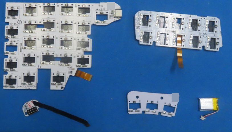
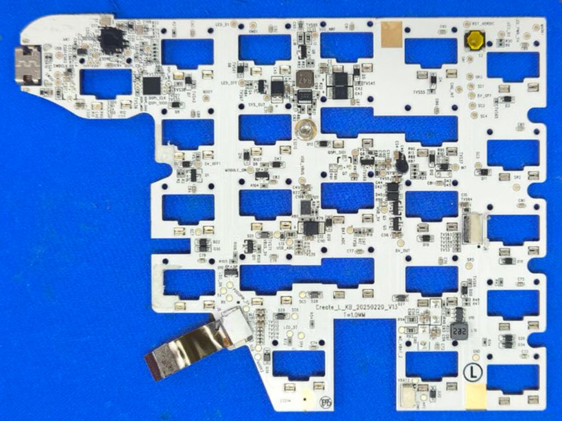
A half has three hinged sections (body, wing, dock) and four boards: the mainboard under the body, a
wing board, a dock (thumb-key) board and a small pogo board carrying the dock contacts
DOC14. The mainboards are Create_L_KB_20250220_V13 (left) and
Create_R_KB_20250221_V13 (right), 1.0 mm thick (T=1.0MM), with a circled L or R; the left board
shows the same string on both faces DOC CRL IP1 p8, p9; CRR IP1 p612. The full board list is on Board inventory.
The SoC is an nRF52840
The radio SoC (U2) in both halves is a Nordic nRF52840 in the CKAA package (wafer-level chip-scale,
about 3.5 x 3.6 mm), build code D0, lot 2301ME. The marking reads N528… / CKAAD0 / 2301ME; the
end of line 1 is partly hidden by the potting edge in the photos DOC INFERRED CRL IP1 p10 (crop re-viewed
2026-09-23), CRR IP1 p812.
Why nRF52840 and not nRF52811, without relying on line 1:
- CKAA is an nRF52840 package code; the nRF52811 codes are QFAA, QCAA and CAAA DOC.
- Conducted peak output reached 8.2-9.3 dBm at power setting 8, above an nRF52811's +4 dBm maximum DOC INFERRED CRL BLE report p10, p131.
- Each half enumerates USB with no second MCU on either face, and the nRF52840 has native USB DOC INFERRED.
- Keyboard images are 218 064 to 361 632 bytes in 663 552-byte bootloader slots, far beyond an nRF52811's 192 KB flash STATIC10.
- The dongle's clearly marked nRF52840 carries the same lot,
2301MEDOC3.
Coded-PHY support (the FCC reports test 125 kbps S=8) does not tell the two parts apart: both support it. It only rules out parts such as the nRF52810 DOC INFERRED1.
The nRF52840 has 1 MB flash, 256 KB RAM, a full-speed USB 2.0 device, a QSPI controller and a CryptoCell security core; the firmware images are decrypted on the device during the bootloader swap, so the host never holds a key DOC STATIC7. See Firmware images.
The SoC and the flash sit at the rear-inner corner next to the USB-C port, under a cut-out in a white foam layer, not in the middle of the board DOC CRL IP1 p8-p10; CRR IP1 p812.
Flash and clocks
- External flash (
U1). A Winbond serial NOR flash in a leadless 8-pad package about 4 mm square (not SOIC-8), on the nRF52840's QSPI bus; part number and capacity are not legible DOC CRR IP1 p8 (winbondwordmark), CRL IP1 p921. - QSPI test pads beside the flash: left
QSPI_CS,QSPI_CLK,QSPI_SIO0,QSPI_SIO1; rightQSPI_CLK,QSPI_SIO0,QSPI_SIO3and a CS pad DOC (right crop re-viewed 2026-09-23). - Two image families. NayaCore ships two families of keyboard images ("flash generation" A and B,
the
_64files) and picks one by a bit in the USB PID; this may mean two flash parts or capacities exist. Only generation A has been seen on hardware STATIC INFERRED9 (the owner's boards enumerate generation-A PIDs); details on Firmware images. - Clocks.
Y1is a 32.000 MHz crystal markedYC32.0(2016 class); a second two-pad partY2has an illegible lid (a 32.768 kHz crystal is the likely reading) DOC INFERRED CRL IP1 p10; CRR IP1 p8.
Antenna and radio
The antenna is a Boen RF0400A printed meander trace on the mainboard (about 7.8 x 3.2 mm), silkscreen
ANT, at the rear-inner corner beside USB-C, behind the black non-metal end cap. The vendor confirms
the cap is the RF window: the all-metal body blocked the signal, so the antenna was moved next to the
USB-C port under a plastic section DOC CRL ANT p4; CRL IP1 p7; CRR EP p311718.
The vendor sheet gives the RF0400A 0.8 dBi peak at 2400 MHz (the filed value); across 2400-2480 MHz its gain is -0.3 to 0.8 dBi and its efficiency 46.1-63.0 %. The sheet's "Directivity" column equals minus the efficiency in dB, so that column is mislabeled INFERRED. The left half's RF-exposure report (R00, never revised) still files 0.59 dBi, the sheet's 2460 MHz value; the R01 reports switched to 0.8 dBi DOC CRL ANT p1; CRL BLE p11; CRL MPE p41.
| Radio as tested | Left half | Right half | Evidence |
|---|---|---|---|
| PHYs | BLE 1M, 2M and coded 125k (S=8), 2402-2480 MHz, GFSK | same | DOC BLE reports p1012 |
| Maximum peak conducted output | 9.30 dBm (2M), 8.5 mW | 8.36 dBm (2M), 6.9 mW | DOC (text layers verified 2026-09-23) |
| Maximum average output | 7.14 dBm (1M) | 7.25 dBm (1M) | DOC |
The manual gives Bluetooth 5.4; the Bluetooth SIG listing's core-spec field reads 5.1 and references Zephyr's host and nRF52 controller designs DOC46. Each half's filing also carries a separate "2.4G SRD" 2 Mbps test report besides BLE DOC; whether shipping firmware ever uses that mode is OPEN (details; see Regulatory records).
USB, debug pads and reset
- USB-C. One unmarked USB Type-C receptacle (
USB1) per half at the rear-inner corner, facing the other half; whether it is a 16-pin or 24-pin part is not resolvable DOC CRL IP1 p6-p9; CRR IP1 p8. - Debug and test pads at the USB-C corner: left
SWDIO,SWDCLK,TP1,TP7,USB,D+; rightSWDIO,SWDCLK,TP2. A re-view of the right-half crop on 2026-09-23 also shows aD+label and one beginningUS, so the two halves most likely carry the same set. NoD-label is visible in any crop DOC INFERRED CRL IP1 p7, p9; CRR IP1 p812. - Debug lock. Whether the SoC's debug port is locked (APPROTECT) on shipped halves is unknown; build code D0 fits Revision 2 silicon, while the hardened Revision 3 uses a different code INFERRED (details).
- Reset. A tactile switch
S2with a yellow cap beside a pad labeledRST_NORDIC, plus aBOOTpad (possiblyBOOT1) DOC CRL IP1 p9; CRR IP1 p7. - Protection. Many unmarked ESD and TVS parts (
ESD1-ESD11,TVS...) sit around USB-C and VBUS DOC CRL IP1 p7-p10; CRR IP1 p8.
Power parts and rails
The power parts are unread: a 0.47 uH inductor (R47, L11) and a 2.2 uH inductor (2R2, L10),
each next to an unmarked converter IC; a square QFN near the USB_ADC, BAT_ADC, VBUS_5V and
CHG_?NT pads (a charger or power manager, inferred); SOT-23 load switches (one marked S2U); two
polarized bulk capacitors; one potted glob DOC INFERRED CRL IP1 p9; CRR IP1 p8. Rail and sense pads on the
mainboard: VBUS_5V, USB_ADC, BAT_ADC, SYS, SYS_OUT, 5V_OUT, 5V_OFF, 5V_OFF1,
MODULE_ON, LED_PWR_5V, LED_OFF, LED_01, LED_02, INT and grounds; their roles (switched
module, LED and 5 V rails; ADC sense points) are read from the names DOC INFERRED. The cell connects at a
receptacle on pads VBAT2, NTC and (probably) MZ_VBAT_2, for the cell's three-wire lead (red,
white, black; the white wire is most likely an NTC or ID line) DOC INFERRED CRL IP1 p9; CRL IP2 p14. See
Power and batteries.
Per-key lighting and the key matrix
- LEDs. Each mainboard carries 24 addressable 4-pad RGB LEDs, daisy-chained with no LED driver IC; the parts are unmarked (WS2812/SK6812 class is a reading from the footprint) DOC INFERRED CRL IP1 p8, p9; CRR IP1 p6.
- Matrix. Test pads
SR1-SR5(rows) andSC1-SC6(columns); one small diode per key (D3-D47); the dock board continues the scheme (SR*_2,SC8_2) DOC INFERRED CRL IP1 p9; CRL IP2 p16. The exact wiring is not recovered. - Keyscan bypasses the split link. Key-matrix events can be read straight from each half with the keyscan command: 143 events from a right half that was not typing through the left MEASURED (owner's board, 2026-09-20, during a firmware mismatch). See Command map.
- Sockets. The mainboard carries 24 hot-swap key positions (two socket pads per window) DOC.
- The LED map. The whole-board LED map has 136 entries per layer (0-73 keys, 74-87 the two light bars, 88-111 and 112-135 the two module-bay blocks); the left half drives both halves' LEDs from it. Per half, 24 + 10 + 3 key LEDs plus 7 bar LEDs make 44; two halves make 88 = indices 0-87 MEASURED DOC INFERRED (owner's board, 3.41.0, 2026-09-08; a second board, 3.28.7, 2026-09-19). Details on Layout and positions and LEDs.
- Campaign count. The 2023 campaign promised "90 individually addressable RGB LEDs" in zones of 68 (body), 6 (dock edge) and 10 (wing indicators), which add up to 84; the shipped board has 44 key and light-bar LEDs per half (88 in all) DOC INFERRED12.
Board-to-board links
A flip-lock ZIF connector takes the wing flex (about 12-14 contacts), and a gold flex of about 12-13
conductors runs to the dock board, exiting beside pads LDO_ON, TX, RX and POGOPIN_5V DOC CRL IP1
p8, p9; CRR IP1 p6, p7.
Wing board, light bar and power switch
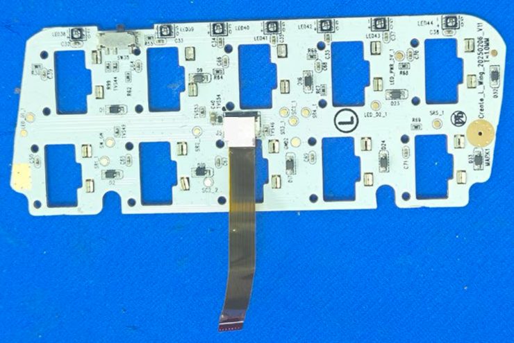
The wing boards are Create_L_Wing_20250206_V11 and Create_R_Wing_20250206_V11 (right middle
hidden), 1.0 mm, with 10 key positions carrying the same designators on both wings (SW1, SW2,
SW9, SW10, SW16, SW17, SW23, SW24, SW32, SW33) and 10 per-key LEDs (LED36-LED45)
DOC CRL IP1 p11, p12; CRR IP1 p9.
The light bar is exactly 7 addressable LEDs in a row along one long edge of the wing board's back face (seen on the right wing; the left wing's back is under black film); in the LED map the two bars are indices 74-80 and 81-87 DOC MEASURED (LED map measured on the owner's board, 3.41.0, 2026-09-08).
The power switch is a right-angle SMD slide switch (unmarked) on the outer end face of each wing; on the right wing it sits between the 6th and 7th light-bar LEDs. Each half has its own switch DOC CRL IP1 p12; CRR IP1 p94. Which slide direction is ON cannot be read from the part: the v1.0.6 manual's drawings disagree, and v1.1.0 draws slide up = ON DOC45. Batch 1 units got "a bit thicker" power switches DOC21. The switch works while USB is connected: switching OFF on USB shuts the half off, and switching back ON restarts it MEASURED (owner's board, 2026-09-23), as the v1.1.0 manual says ("Create will respect the ON/OFF state even while connected over USB") DOC5; see Power and batteries.
Dock (thumb-key) board and pogo board
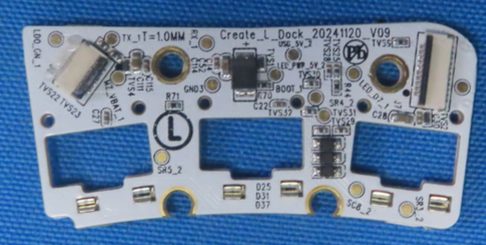
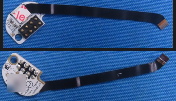
The dock boards are Create_L_Dock_20241120_V09 and Create_R_Dock_20241120_V09, 1.0 mm, about
47 x 21 mm (inferred), under the module bay. Each carries 3 hot-swap thumb-key positions, 3
addressable LEDs, one diode per key (D25, D31, D37), TVS parts on every line and two FPC
connectors (mainboard flex and pogo flex) DOC INFERRED CRL IP2 p16; CRR IP1 p12. Its test pads: TX_1,
RX_1, BOOT_1, MZ_VBAT_1, LDO_ON_1, USB_5V_2, GND3; matrix SR1_2, SR3_2, SR4_2,
SR5_2, SC8_2; LED LED_D7_1, LED_PWR_5V_2. There is no D+ or D- anywhere DOC.
The pogo board, Create_L_PogoPin_20250109_V10 (0.6 mm), carries the half's 8 dock spring pins and
hangs on a black flex of about 50 mm to the dock board DOC CRL IP2 p15. Detail on
Module dock.
Switches and sockets
The switches are Kailh CPG-1232, which is Kailh's PG1232 "Choc Mini" low-profile switch, in the 0.45 x 0.42 mm pin variant; Kailh lists the PG1232 at 14.5 x 13.5 x 8.2 mm with 2.4 mm travel. There are 37 per half, 24 on the body, 10 on the wing and 3 on the dock, 74 in total DOC48. They sit in hot-swap sockets (two slotted pads per key; the socket part is not legible, PG1232-compatible inferred) DOC INFERRED4. The lab samples carry red-stemmed switches with clear housings; the switch type was a purchase option (the 2026 shop listed Clicky, Linear, Tactile, Silent Linear and Silent Tactile packs) DOC CRL IP1 p5, p6; CRR IP1 p511.
Switch history: Gateron KS-28 in the 2023 campaign; Kailh PG1232 adopted in March 2024 (the promised KS-28 hot-swap socket never came, and the KS-28 had quality problems); the dock keys moved from Kailh CPG1316 scissor switches to PG1232 in September 2024, about 3 mm taller, making every key hot-swappable with one switch type; Batch 0 came with linear switches, Batch 1 with tactile, and linear was the default from 2025-06. The campaign gave an 11.2 mm typing height for the main keys and 9 mm for the dock keys DOC1215181922.
Keycaps
Keycaps are polycarbonate, individually sculpted, each labeled on its underside with a coordinate
(LA1...RH4); the keyboard takes only its own keycaps (vendor, 2023). The 2023 campaign specified
backlit ABS shine-through keycaps; polycarbonate and PC-ABS were sampled in 2024
DOC4241216. Larger keycaps have wire stabilizers; the manual does not
say which keys. NayaFlow draws two tall inner keys (LH1, RH1) and two wide space keys (LE5, RE5)
DOC STATIC49. The vendor showed US QWERTY, German, JIS and blank keycap layouts DOC11.
Enclosure
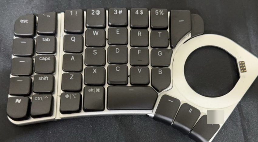
- Materials. Body, dock and wing are "Aerospace Grade Aluminum" (the alloy is not stated); the dock's underside plate is black, material unknown; a black non-metal end cap carries the USB-C port DOC42.
- Machining. The body is built from 10 custom CNC-machined parts (20 operations); each hinge is press-fitted into two machined blocks DOC23.
- Plates. Separate rigid metal switch plates for the body (24), wing (10) and dock ring (3), butted at seams with screws and linked only by flex; the hinging is in the case. The PCBs float on foam ("foam-suspended PCB for sound dampening") DOC CRR IP1 p5; CRL IP1 p5, p64.
- Tenting. Two torque hinges per half (a round pivot on the wing, two knuckle assemblies on the dock), up to 27° DOC41325.
- Underside. 12 silver screws matching 12 screw symbols on the label outline, at least 13 small black
screws around the dock ring plate, raised foot strips (body 2 curved, wing 2 short plus 1 long, dock
1 plus a small pad), and a filled
LorRcircle near the lower dock hinge DOC21. - Engraving. The Naya "N" logo with "Naya Create" (registered mark), "Designed by Naya in the Netherlands", "Made in China"; the regulatory block sits on the wing's underside plate, rotated 90° DOC21. See Regulatory records.
- Size and weight. The manual gives 212 x 118 x 18 mm and 1.4 kg; the size fits one half (the 1:1 label outline of one half is about 210 x 121 mm, inferred); whether the weight is per half or per pair is not stated. The 2023 campaign spec sheet gave 205 x 120 mm, 17 mm total height and 225 g per half (pre-production) DOC INFERRED4212.
- Batch changes. Batch 0 testers reported loose body screws and switches loose in their sockets; Batch 1 tightened socket tolerance and changed the rubber feet and laser-etch color DOC2021.
Magnets
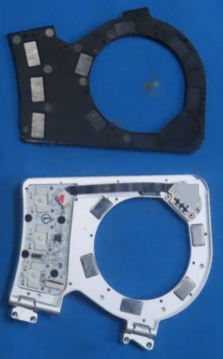
Each half's module bay holds 6 magnets, one on either side of the contact block and 4 more spaced around the circular bay (a steel paper clip is attracted at those 6 points), so the half side is magnetized, not a plain steel strike plate MEASURED (owner's board, 2026-09-23). Mapped onto the FCC photos: the two small features flanking the contact block on the dock chord and the 4 blocks on the black carrier plate are the 6 magnets; the 5 rectangular blocks on the metal bay bracket (a frame with a circular opening and two hinge lugs) did not attract the clip, so they are not magnets MEASURED DOC INFERRED CRL IP1 p5; CRR IP1 p5; CRR EP p2-p312.
Each module's base holds 6 rectangular metal blocks or plates (Tune, Touch, Track); whether those are magnets or steel is not tested (the half side is magnetized, so steel would be enough). The manuals say there are magnets both in the dock and on the module's bottom DOC14 (details).
The two halves also attach to each other back to back magnetically, for storage and transport; the vendor suggested those magnets for DIY mounts, as there are no mounting holes. The switches themselves are not magnetic; the magnets are for modules (vendor, 2023) DOC45121426. The dock opening is a circular through-cutout with one straight chord where the contacts sit; modules are removed by pushing up through the cutout DOC24.
What a port of open firmware would need
The bootloader banner names MCUboot 9ddeffa8169c and Zephyr v3.7.0-5411-g31fea97e05fd MEASURED (owner's
board, 3.41.0, 2026-09-08). That Zephyr hash is an upstream Zephyr main commit of 2024-10-25 (between
v3.7.0 and v4.0.0), not an nRF Connect SDK tag, and the MCUboot hash is in no public MCUboot repository
(a vendor-local build) DOC INFERRED.
Not everything needed for a port of open firmware is known: the board definition (matrix pin-out, LED chain, split-link and dock protocol) sits in the encrypted firmware and is not recovered, and stock MCUboot boots only images signed with Naya's RSA-2048 key, so a custom build needs the bootloader replaced over SWD, whose lock state is unknown STATIC INFERRED. Detail on ZMK and Bootloader.
Safety
Opening a half
Opening a half exposes a Li-ion cell on a three-wire lead: do not short or puncture it (manual). The SWD pads are not a recovery path to try casually: the lock state is unknown, and an SWD erase would remove the stock bootloader and its key (see ZMK). Untested by us.
Open questions
- OPEN QSPI flash part number and capacity; whether generation B uses another part (details).
- OPEN The half's power tree: charger, DC-DC ICs, load switches, the potted part (details).
- OPEN Cell connector pin count and which wire is the NTC (details).
- OPEN Whether
Y2is a fitted and used 32.768 kHz crystal (details). - OPEN LED part number and protocol (details).
- OPEN SoC silicon revision and debug-lock state (details).
- OPEN Slide switch part and ON direction; socket part (details); USB-C pin class (details).
- OPEN Whether the module-base blocks are magnets or steel (details).
- OPEN Which light bar is indices 74-80 (details).
Sources
-
FCC ID 2BQ4V0825CRL (left half; the module photos are in both filings): exhibits on the FCC record (FCC EAS search, grantee 2BQ4V; mirror fccid.io/2BQ4V0825CRL). Codes such as "CRL IP1 p10" are explained on Regulatory records. ↩↩↩↩↩↩↩↩↩↩↩↩↩↩↩
-
FCC ID 2BQ4V0825CRR (right half), including the label artwork; mirror fccid.io/2BQ4V0825CRR. ↩↩↩↩↩↩↩↩↩↩↩↩
-
FCC ID 2BQ4V0825DG (dongle); mirror fccid.io/2BQ4V0825DG. ↩
-
Naya Create User Manual Version 1.0.6, FCC ID 2BQ4V0825CRR user manual exhibits (fccid.io); see Manuals. ↩↩↩↩↩↩↩↩↩↩↩↩↩↩↩
-
Naya Create User Manual Version 1.1.0 (vendor PDF, 2025-11-10); see Manuals. ↩↩↩
-
Bluetooth SIG qualification listing 311198 (listing search), read 2026-09-23. ↩
-
Nordic Semiconductor, nRF52840 Product Specification. ↩
-
Kailh product data for the PG1232 low-profile switch. ↩
-
NayaFlow 1.25.1: NayaCore 6.11.0 strings (
setCreateFlashGenerationFromPid) and the renderer's key geometry (static reading). ↩↩ -
create-legacy-firmware,
FIRMWARE-HISTORY.md(image catalog of the 25 stable releases). ↩ -
The vendor's former website and shop images, archived by the Wayback Machine (naya.tech captures); cited only, images not reproduced. ↩↩
-
Kickstarter campaign page with its Specs Sheet and FAQ, naya-create/naya-create (2023). ↩↩↩↩↩
-
Kickstarter update 6, 2023-09-28. ↩
-
Kickstarter update 11, 2024-02-15. ↩
-
Kickstarter update 12, 2024-03-01. ↩
-
Kickstarter update 13, 2024-05-08. ↩
-
Kickstarter update 14, 2024-07-24. ↩
-
Kickstarter update 15, 2024-09-03. ↩↩
-
Kickstarter update 17, 2024-11-04. ↩
-
Kickstarter update 19, 2025-02-11. ↩
-
Kickstarter update 20, 2025-03-19. ↩↩
-
Kickstarter update 21, 2025-06-16. ↩
-
Kickstarter update 22, 2025-07-28. ↩
-
Reddit, vendor comment jkqzcq4 (2023-05-19); archived text, not live-verified. ↩
-
Reddit, vendor comment jn3t9dt (2023-06-06); archived text, not live-verified. ↩
-
Reddit, vendor comment j35i18k (2023-01-06); archived text, not live-verified. ↩